An Inside Look at High-Speed ADC Accuracy, Part 3
This file type includes high-resolution graphics and schematics when applicable.

Signal-chain accuracy analysis can be an overwhelming task to understand in any design. In Part 2, many errors were discussed that accumulate throughout the signal chain and are eventually “seen” by the converter. Remember, the converter is the bottleneck of the signal chain and ultimately decides how “accurate” the signal can be represented. Therefore, choosing the converter is key to setting the overall system requirements. In this article, the focus will continue to build on this knowledge, analyzing the types of dc errors that can accumulate throughout the given signal chain.
Two types of errors can accumulate through a signal chain—dc and ac. Errors that are dc or “static,” such as gain and offset, provide an understanding of the signal chain’s accuracy or sensitivity. Errors of the ac variety, otherwise known as noise and distortion, set the bounds on performance and dynamic range of the system. Both are important to understand because they both ultimately determine the resolution of the system.
This article will specifically analyze dc errors, breaking down each inaccuracy as it relates to both passive and active devices. A matrix or spreadsheet will be developed to show how to “add” or accumulate error throughout the signal through different methods.
For ac errors, refer to references 1 and 2. Here, a review of noise basics, such as bandwidth summation and error accumulation from an ac perspective, can determine the overall SNR of analog signal-chain design.
Signal-Chain Recap
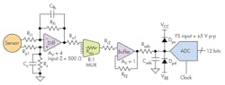
From Part 2, the goal was to design a simple data-acquisition system that could meet 0.1% accuracy (Fig. 1). Meaning for every 1-V input, the output would be either 0.99388 V or 1.00612 V. Therefore, the converter was defined to have a capable dynamic range of 60 dB or 9.67 ENOB, assuming a 10-V full scale. It has two stages of amplifiers, a multiplexer, and an analog-to-digital converter (ADC). The sensor, cables, connector(s), printed-circuit-board (PCB) parasitics, and any outside influences/errors will be neglected in this analysis since this can depend heavily on the application or signal the designer is trying to measure.
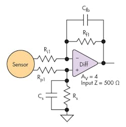
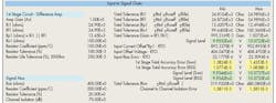
To define references for each error, each stage for the analysis should be broken down into individual sections. The first stage of the data-acquisition signal chain is a simple difference amplifier (Fig. 2). The amplifier has a gain of 4× and input impedance of 500 â¦. The capacitors are in place for optional filtering purposes.
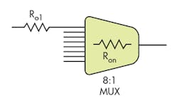
The difference amplifier’s output signal is then applied to one of the eight inputs of the multiplexer (Fig. 3). Each input is “buffered” with a damping resistor (Ro) to minimize charge kickback from the multiplexer’s channel switching. Each channel internally will have some parasitic or characterized Ro per the multiplexer’s datasheet specifications.
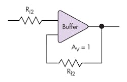
The resulting channel signal is then applied to a unity-gain buffer-stage amplifier (Fig. 4). The resistors are applied to minimize input bias current imbalance.
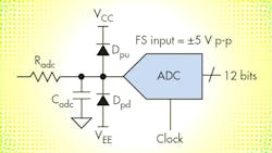
After the signal is buffered, it’s applied to the 12-bit, 1-Msample/s ADC, where it then finally enters the digital domain (Fig. 5). The series resistor is applied to buffer or dampen the signal between the amplifier and converter, adding source resistance between the two devices. This minimizes charge kickback from the converter to the amplifier, much like the multiplexer. This also helps the amplifier output settle and prevents it from oscillating.
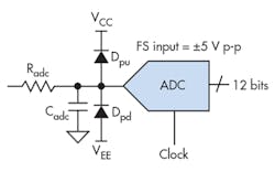
The capacitor provides a simple low-pass anti-aliasing filter (AAF) to attenuate signals and noise outside the band of interest. The design of the AAF depends greatly on the system’s design and application. Lastly, the pull-up and pull-down diodes add input protection against any fault conditions of extreme signal overload conditions that may be applied to the converter’s input.
Now that all of the signal-chain components have been defined, let’s start looking at the errors associated with each stage. In the following sections, both passive and active errors will be review based on each of the signal chain’s stages discussed here.
DC Passive Errors
All passive components have errors associated with them, especially resistors. Resistors seem like simple devices, but they can cause error throughout any signal chain if not specified correctly for the design. Choosing the right type of resistor and its composition isn’t covered here. Keep in mind, though, that depending on the application, some resistor types maybe more well-suited than others.
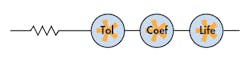
Resistive dc errors result from non-ideal resistor tolerances. Simply specifying the value tolerance isn’t enough. However, being overly critical about resistor error tolerances can also yield diminishing returns and overcomplicate the analysis. At least four critical specifications need attention when specifying a resistor type for a given signal chain:
1. Value tolerance, usually specified in %.
2. Temperature coefficient or drift, usually specified in ppm/°C.
3. Life drift or qualification, usually specified in % over a set amount of hours (usually in 1000s).
4. Value tolerance ratio, value tolerance specified in % when two or more resistors are present in a network or the same package and are matched in value.
To give an example of how resistor errors can accumulate (Fig. 6), let’s look at the following: A 100-⦠resistor with a value tolerance of 1%, drift of 100 ppm/°C, and life tolerance of 5% will yield a resistance from 93.15 to 106.85 ⦠over a 5000-hr. life within an 85°C temperature range:
Total Tolerance (Rvalue + Rtol + Rcoeff + Rlife) = (Rvalue + ((Rtol/100) * Rvalue) + (((Rcoeff * 0.000001) * TempRange) * Rvalue) + ((Rlife/100) * Rvalue)) = 94 to 106 â¦.
Hard-to-Find-Information Side Note: Some components have a life specification of only 1000 hours. Yet, the design may call for a much longer time, say 10,000 hours. To get around this, don’t multiply the 1000-hr. figure by 8.77 (8766 hours/year); it’s much too pessimistic. Long-term drift in any precision analog circuit is going to have some amount of “random walk” to it. It’s more correct to take the square root of this number or √(8.766) = ~3 times the 1000-hr. figure. Therefore, a 10,000-hr. life number is √(10.000) = 3.16 * 1000-hr. specification and so on.
It should be noted that capacitors and inductors have errors, too. However, these errors are usually negligible and add no substantial value for this type of dc analysis. These devices are also reactive in nature and have the greatest impact on filtering and bandwidth tolerances, which again isn’t applied in this particular dc analysis.
DC Active Errors
The signal chain described in Figure 1 has the most common building blocks, which describes one approach to implementing a data-acquisition system. It consists of two amplifiers, a multiplexer, and an ADC. Keep in mind, however, that many types of active devices describe all sorts of signal chains and different system topologies. All active devices will have some sort of dc error(s) when implementing this type of analysis. It’s important to decide which of these errors need to be taken into account to understand the accuracy of the system under design.
Basically, two types or groups of errors are involved in dc accuracy. These errors are individual and global to all active devices. Individual active device errors will exhibit its known dc error relative to that device only. Such errors can be found in their respective datasheets. For example, input offset voltage of an amplifier would be considered an individual error because this error is particular to this active device only.
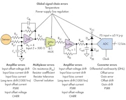
Global errors are common to each of the active devices in the signal chain or system by the same amount, but exhibit a different error based on the active device’s individual performance (Fig. 7). A global-error example would be line regulation of the bus’s supply and temperature. Now, let’s break down each of these errors for the three active devices shown in the signal chain.
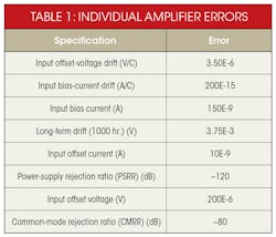
It’s well-known that amplifiers are still far from ideal. They have many errors that are commonly listed in the datasheet. Offset voltage and bias current are two common errors, but it’s also important to include any drift errors, long-term errors, and isolation errors such as power-supply rejection ratio (PSRR). Table 1 shows a listing of the following errors that should be considered when using amplifiers.
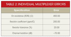
Multiplexers typically have fewer errors than an amplifier. The “on” resistance and channel isolation are the most influential multiplexer dc errors. Table 2 lists the errors that should be considered when using multiplexers.
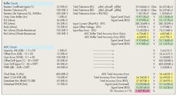
Converter errors were specifically reviewed in the first part of the series. Offset, gain, and DNL are well-known and understood. It’s important to include power-supply sensitivity as well, or PSRR. The following list of converter errors should be considered when using ADCs from Part 1:
• Relative accuracy, DNL, which was defined as ±0.5 LSBs.
• Relative accuracy tempco, DNL tempco, which is typically included in the relative accuracy specification in the datasheet.
• Gain tempco error, which was ±2.5 LSBs (from the example above).
• Offset tempco error, which was ±1.3 LBs (from the example above).
• Power-supply sensitivity, which is typically in the form of low-frequency PSRR within the first Nyquist zone; this can typically be expressed as 60 dB or ±2 LSBs for a 12-bit ADC.
To keep the article at a reasonable length, this discussion will not go into the details on how each of these errors is derived within the active device itself. All of these errors are well-defined and described in various papers and texts. What’s important to note here is that all of the essential errors have been considered so that the analysis is robust enough to meet the system’s accuracy target specifications.
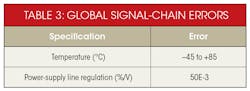
Individual active device errors have been suggested and defined. Now global errors should be considered which influence the signal chain as a whole (Table 3). In this simple example, only temperature and line regulation will be factored into the analysis as global errors. However, it is important to add any other outside influences that maybe inherent to the particular application or design.
Putting It All Together
Now that all of the errors have been defined both actively and passively, it’s time to put them into a spreadsheet to calculate dc accuracy of the signal chain. Table 4 shows one such approach to accomplish this task.
Even though there are many ways to go about analyzing signal-chain accuracy, using the spreadsheet method offers the greatest flexibility. It also provides a solid understanding on how to go about “crushing” all of these error numbers down within the signal-chain design. This method allows the designer to make quick and effective tradeoffs between many suitable devices that maybe considered for the design.
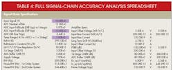
Take the time to produce a spreadsheet that has good layout and is orderly. At the top, global errors and signal-chain specifications are defined because these numbers affect the performance of the signal chain as a whole. The amplifier specifications/errors were also placed at the top, since there are many errors and two amplifier stages throughout the signal chain.
Continuing down, on the left-hand side of the spreadsheet, all of the errors are divided down into each circuit stage. The resistor errors were also grouped with each stage to understand the tradeoffs accordingly. The right-hand side shows a continuous calculation and accumulation of error as the signal flows to and from each stage.
In the calculations, all of the errors are put into a voltage format. This makes it easier, since the converter is at the end of the signal chain and has an input full-scale described in voltage. RTO (refer to output) is used to describe the continuous accumulation of errors from one stage to the next. Each stage also produces a separate “Sum” total and “RSS” (root-sum square) total to show how the errors are accumulating, depending on the method used.
Therefore, the end result in Table 4 above shows a total accumulation of ±2.6% summed error and a ±1.6% RSS error. This is for the entire signal chain discussed throughout this article, given the datasheet specifications for each part and the global conditions stated above at 26°C.
Total Accumulation
Accuracy can be calculated in many ways and can take on many forms. Depending on how this is viewed by the designer, it should be understood and documented to avoid creating any misrepresented results. Remember from Part 1, simply taking the root-sum-square (RSS) of all these error sources might seem overly pessimistic. Yet a statistical tolerance maybe overly optimistic (the total sum of errors divided by the number of errors). Finding the actual tolerance of the entire signal-chain error should be somewhere between these two thoughts or methods.
Therefore, when adding (accumulating) accuracy errors in the entire signal chain, or any accuracy system analysis, the designer could use a weighted-error-source approach (as shown in the ADC example in Part 1), then RSS these error sources together. This will provide the best method in determining the entire signal chain’s overall error.
Conclusion
Many errors occur with both passive and active devices. Not all are important, but keep in mind those that are important to the signal-chain application at hand. Not all errors may be valid for every application. Deciding which errors are the most dominant or have the most influence or “weight” is essential to any dc accuracy error analysis. A spreadsheet was developed to show how the signal-chain example in this article meets the requirements of <±2.0% accuracy. For a copy of this spreadsheet, email me at [email protected], or contact me at Analog Devices Engineering Zone.
Choosing the right passives can make just as much a difference in the total accumulated error in the signal chain as well as the active devices. Creating and partitioning a spreadsheet makes it simple and tidy to consider many different devices and tradeoffs quickly. Finally, accumulation of error can take on many forms, and the most common practice used is the RSS accuracy method.
However, some may argue that a weighted summation approach of errors is the right way to determine a true “worst-case dc error.” If not, this can easily cause a signal chain to be over-designed, leading to more parts to compensate for the original set of errors. Not to mention the increase in cost and the design’s size, weight and power (SWaP).
References:
1. MT-230: “Noise Considerations in High-Speed Converter Signal Chains,” Analog Devices Inc.
2. “Noise considerations in high-speed converter signal chains,” DSP – FPGA – August, 2013.
Further reading:
Kaiser, Cletus J., The Resistor Handbook, 2nd Edition, 1-11.
MIL-PRF-55342H
Kester, Walt, The Data Conversation Handbook, Analog Devices Inc.
Jung, Walter G., IC Op-Amp Cookbook, Third Edition.
AN102: “Errors, What Are They And How Bad Can They Be?,” Dataforth Corp.
AN504: “SCM5B, Interpeting Drift Specifications,” Dataforth Corp.
AN-539: Nash, Eamon, “Errors and Error Budget Analysis in Instrumentation Amplifier Applications,” Analog Devices Inc.
Nash, Eamon, “A Practical Review of Common Mode and Instrumentation Amplifiers,” Analog Devices Inc.
Irvine, Robert G., Operational Amplifier Characteristics and Applications , 3rd Edition.
About the Author

Rob Reeder
Application Engineer, High-Speed Converters, Texas Instruments
Rob Reeder is currently the application engineer for High-Speed Converters at Texas Instruments (TI) in Dallas. Rob’s prior experience includes RF design at Raytheon Missile Systems in Tucson, Ariz., including analog receivers and signal-processing applications. He was also a system application engineer with Analog Devices in the High-Speed Converter and RF Applications Group in Greensboro, N.C., for over 20 years.
He has published over 130 articles and papers on converter interfaces, converter testing, and analog signal chain design for a variety of applications. Rob received his MSEE and BSEE from Northern Illinois University in DeKalb, Illinois, in 1998 and 1996, respectively. When Rob isn’t writing papers late at night or in the lab hacking up circuits in the lab, he enjoys hanging around at the gym, listening to EDM, building rustic furniture out of old pallets, and, most importantly, chilling out with his family.
Comment About the Article
To join the conversation, and become an exclusive member of Electronic Design, create an account today!

Leaders relevant to this article: