Download this article in .PDF format
This file type includes high-resolution graphics and schematics when applicable.
Today, almost every electronic product contains an analog-to-digital converter (ADC). When designing a new product, one of the first decisions is deciding on the type of ADC. With multiple types to select from, your choice is critical because it could very well determine the overall success and performance of your product. This article can help in the selection process as it explores two of the most popular types.
Literally dozens of different specifications are used to define ADCs. Among the most important are:
Resolution: Resolution is the number of possible output bits that an ADC can generate per conversion. Resolution is also the smallest analog increment corresponding to a one LSB converter change. Moreover, analog resolution determines the smallest analog input signal that can be represented.
Accuracy: Related to resolution, accuracy reveals how close a converter output comes to representing its maximum possible theoretical resolution. Accuracy of an ADC is determined by the quantization noise, nonlinearities in the transfer function, and by additional sources of noise in the ADC.
Sampling speed: Sampling speed is the highest number of conversions that can be made per second. For example, an ADC may be able to output 10 million samples per second (10 Msamples/s). Sampling speed is related to conversion time or the period of time it takes to output one conversion. The conversion time or speed of a 10-Msample/s ADC is 100 ns.
Quantizing noise: Quantizing noise is an unwanted voltage added to the input signal—it’s the error that occurs during the conversion. More specifically, it’s a sawtooth-shaped noise signal that’s the difference between the actual input value and the voltage represented by the digital codes possible in the converter. The peak noise value is the least-significant-bit (LSB) analog resolution value. This value is VR/2N, where VR is the converter reference voltage and 2N is the number of resolution bits. Quantizing noise reduces as number of resolution bits increases.
There are multiple other specifications too complex to discuss in this short article, but more detail can be found in this reference.
Comparing Types of ADCs
Five main types of ADCs are commonly used: dual slope, successive approximation, flash, pipelined, and delta-sigma. The dual slope, used mostly in measurement instruments such as a digital voltmeter, has a slow sampling rate. Successive-approximation ADCs have good resolution and moderately high sampling rate, while the flash converter offers the fastest sampling but typically has lower resolution. The pipeline converter employs multiple flash converters to extend the resolution but retain high speed. Finally, the delta-sigma (ΔΣ) offers very high resolution, but lower sampling speed. Table 1 shows the relative characteristics of each type.
Two of the most popular types are the SAR and delta-sigma. The remainder of this article compares and contrasts these two types in more detail.
The SAR Converter
The successive-approximation converter is one of the oldest and most widely used types of ADC. It’s commonly found in data-acquisition, industrial-control, and instrumentation applications, where ultra-high speed isn’t necessary.
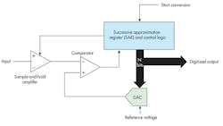
Figure 1 shows the design of a successive-approximation ADC, at the heart of which is the successive-approximation register (SAR). The converter output is taken from this register in parallel. The parallel output also feeds a digital to analog converter (DAC), which may use a resistive or switched-capacitor network to generate a stepped analog output based on the SAR content. A regulated, fixed dc reference-voltage input to the DAC sets the converter’s input voltage range (e.g., 0 to 5 V).
The DAC output is one input to a comparator, with the other being the analog signal to be digitized. This input signal is usually pre-conditioned by a sample-and-hold (also called a track/store) amplifier. The S/H amp contains a switch and a capacitor that continuously charges/discharges to the input voltage. At the start of a conversion, the switch opens and the most recent input value is stored. The S/H amp “samples” the input voltage, and ensures that the voltage at the input to the comparator is constant during the conversion process.
Some applications may not need the S/H amplifier. For lower-resolution and lower-sampling-rate applications, the ADC may be adequate.
The resolution of the ADC depends on the number of bits in the SAR. SAR IC converters are available in sizes from 8 to 18 bits—the greater the bit count, the greater the resolution and accuracy. For example, for a 12-bit SAR and a 5-V DAC reference, the converter can resolve an analog value as low as VR/2N = 5/212 = 5/4096 = 1.22 mV.
Converter operation centers around the special algorithm used by the SAR. Unique control logic sets or resets the individual flip-flops in the SAR one bit at a time according to the comparator’s output state. The SAR is initially reset. When a start conversion input signal is received by the control logic, the most significant bit (MSB) of the SAR is set and a comparison is made. If the input voltage is greater than the DAC output, the MSB remains set; otherwise the MSB is reset.
The next MSB is then set and another comparison is made. The clock signal determines the rate of setting and resetting the SAR bits. The process continues until all bits are evaluated. Total conversion time is the clock period times the number of SAR bits. For a 16-bit SAR and a clock speed of 2 MHz, the conversion time is 16 × 0.5 µs = 8 µs. This represents the converter’s fastest sampling rate.
At the end of the conversion, the digital value of the analog sample taken at the input is in the SAR and can be read directly in parallel. Alternately, the SAR content may be transferred to a shift register that can shift the digital value out serially.
The Delta-Sigma Converter
The delta-sigma (ΔΣ) is a newer design that was developed when digital signal processing (DSP) became practical. It’s unique and complex, but offers the benefits of greatest resolution of any ADC plus noise mitigation. However, it’s slower than most other ADCs, so its applications are usually restricted to dc and audio frequencies. Typical applications are instrumentation and digital audio (e.g., CDs, MP3, etc.)
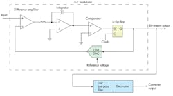
Figure 2 shows the basic organization of a ΔΣ converter, with the main circuit called the “modulator.” The input signal is applied to a differential amplifier that subtracts the DAC output. The difference value is then integrated and the output result is compared to ground. The comparator output sets or resets the D flip flop (FF) accordingly. The state of the D FF is sent to a 1-bit DAC whose output is either the reference voltage or zero.
Alternately the DAC may output a ± reference, such as ±1 V. Such a feedback-loop arrangement produces a serial pulse train from the D FF. This binary output produces a series of binary 1s whose density is proportional to the input voltage level. Each clock pulse generates one sample of the input and one serial output bit. The clock rate is typically much higher than the frequency content of the input signal, which is otherwise referred to as oversampling.
In this state, the serial output is not useful. Instead, it’s further processed in a DSP low-pass filter and a circuit called a decimator. The actual process is beyond the scope of this article, but the result is a sequence of fixed bit-length words representing samples of the input signal to be digitized. The digital filter and decimator are usually integrated as one unit in the IC.
A key feature of the ΔΣ ADC is that the low-pass filter essentially eliminates most of the high-frequency quantizing noise generated by the sampling process. The decimation process reduces the number of output words generated by a factor called the decimation ratio. The decimation ratio determines the number of data samples from the modulator that are averaged together to get each output word. Usually, the greater the resolution, the lower the output word rate.
So Which ADC is Better, ΔΣ or SAR?
The answer is, it depends on your application. Looking at the top two specifications—resolution and sampling rate—which best fits your needs? For highest resolution, go for the ΔΣ, which has up to 32 bits to work with. The SAR is also good, though, with up to 18 bits.
Sampling speed is critical, because the ADC must be fast enough to capture the highest frequency content of the input. Remember the rule that says “sampling frequency must be at least twice the highest frequency content of the input.” This minimum sampling rate is called the Nyquist rate. If input-signal frequency content peaks at 45 kHz, or there are harmonics that must be preserved up to that frequency, the sampling rate must be at least 90 kHz (and usually more). Actually, five to 10 times this highest frequency is even better.
The SAR and ΔΣ converters have a maximum sampling rate to 10 Msamples/s. Keep in mind that the net output data word rate of the ΔΣ is lower than the sampling rate by the decimation factor, and is usually in the kilosamples-per-second (ksamples/s) range. However, the noise reduction will be greater than the SAR.
One benefit of the SAR is that it can be used where multiple inputs must be digitized. A multiplexer placed ahead of the S/H amplifier selects one of the inputs to be converted. The sampling rate of each input is lower by a factor of the number of inputs. For instance, with four inputs and a 5-Msample/s SAR, the maximum sampling rate of each input is 1.25 Msamples/s.
Table 2 is a summary of the characteristics, and lists the pros and cons of the ΔΣ and SAR ADCs. For further details, check out this reference.
About the Author

Lou Frenzel
Technical Contributing Editor
Lou Frenzel is a Contributing Technology Editor for Electronic Design Magazine where he writes articles and the blog Communique and other online material on the wireless, networking, and communications sectors. Lou interviews executives and engineers, attends conferences, and researches multiple areas. Lou has been writing in some capacity for ED since 2000.
Lou has 25+ years experience in the electronics industry as an engineer and manager. He has held VP level positions with Heathkit, McGraw Hill, and has 9 years of college teaching experience. Lou holds a bachelor’s degree from the University of Houston and a master’s degree from the University of Maryland. He is author of 28 books on computer and electronic subjects and lives in Bulverde, TX with his wife Joan. His website is www.loufrenzel.com.


