
Amplifiers are fundamental circuit-design elements.
They drive everything from earbuds to antennas. Placed ahead of analog-to-digital converters (ADCs), they reshape signals from sources as diverse as strain-gauges to ultrasound probes. Through proper selection of feedback passives, they can be configured into high-pass, low-pass, band-pass, and band-elimination filters. Feed them with multiple signals, and they produce harmonic series of all the components of those inputs—good for some applications, a headache in others.
You’d think this venerable component had little left in the innovation department, but it continues to evolve nonetheless. What follows is a review of amplifier basics with a twist. It assumes some engineering knowledge of how transistors are configured into amplifiers, so it will focus more on what’s new and what may not be so widely understood in a universe dominated by digital thinking.
Amplifier ABCs
These ABCs don’t get into how to bias a transistor, but rather how the transistor is operated. It once was a matter of where the device was operated on its transfer curve (Fig. 1). Now, the amplifier class alphabet extends beyond the old classifications.
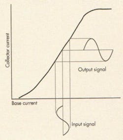
In class A, the active device is biased so that it operates in its linear conduction region during the entire input cycle. In class B amplifiers, there are two devices. The input waveform is split— one active device conducts during half of an input cycle, the other during the other half. Class AB amplifiers resemble class Bs, except they bias their active devices so that both conduct during some portion of the input cycle.
In class C, a single device is biased whereby it conducts during only a small portion of an input cycle. Energy is driven into a high-Q LC tank circuit that continues to ring at its resonant frequency during the portions of the cycle when the active device isn’t conducting. An analogy would be continuously tapping a big bell with a small hammer at a rate equal to the resonant frequency of the bell.
In the beginning, classification had something to say about linearity versus efficiency. Class A amplifiers can be made very linear, but their efficiency is limited. In theory, a class A amp can achieve 50% efficiency with inductive output coupling or 25% with capacitive coupling. Class B amplifiers are subject to “crossover” distortion, but their efficiency is theoretically as high as 78.5%.
Class AB sacrifices some of that efficiency for lower distortion. Class C amps can achieve up to 90% efficiency. The resonance effect of the LC-tuned circuit minimizes distortion. Class B amplifiers are sometimes called “push-pull” because the outputs of the active devices have a 180° phase relationship (Fig. 2). (For a different kind of push-pull configuration, as well as Bridge- Tied Load Amplifiers).
Beyond class C, the simple relationship between alphabetical designations and the input signal’s application to the active device’s transfer characteristic starts to break down. For example, in class D amps there are two devices, as in a class B amp. But they’re driven between saturation and cutoff by a square wave with a frequency significantly higher than the highestfrequency component of the input waveform.
The pulse width or pulse density of the square wave is variable, and one or the other is controlled by the input signal. At the amplifier output, the switching frequency and its harmonics are attenuated by a low-pass filter, leaving only the amplified input waveform.
With field-effect transistors operating most of the time in either cutoff or saturation, losses are primarily from the transistors’ forward-voltage drops. Class D amps can achieve efficiencies as high as 90%, with distortion levels approaching class AB. Suppressing radiated and conducted interference from the switching circuitry is challenging.
Classes E and F are related to class C, since they’re RF amplifier topologies that use LC tank circuits. Where class C amplifiers are widely used below 100 MHz, class E amps are used at VHF and microwave frequencies.
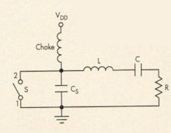
Class E amps differ from class C amps in that the active device is used as a switch, rather than being operated in the linear portion of its transfer characteristic. Figure 3 is an equivalent circuit for a class E amplifier. The switch S represents the active device. L and C are the series-tuned circuit, and R is the load. CS represents all of the parasitic capacitances across the active device, and the choke isolates the power source.
Class F amplifiers resemble class E amplifiers, but use a more complex load network. In part, this network improves the impedance match between the load and the switch. Also in part, it’s designed to eliminate the even harmonics of the input signal so that the switching signal is more nearly a square wave. This improves efficiency by making the switch run at saturation or cutoff longer.
Class G and H amplifiers are variations on the standard class AB. They have additional supply rails that kick in when output signal peaks would otherwise exceed the maximum voltage available from the class AB amplifier’s single voltage rail.
Class G amps feature several power rails at discrete voltage steps and switch between them as necessary. Instead of providing multiple rails, class H amps modulate the voltage on the supply rails in order to track the input signal.
Class G and H amplifiers tend to be used in audio applications. However, a related but almost forgotten alternative called the Doherty amplifier has been revived for cell-phone applications. (William Doherty was an early Bell Labs researcher.)
A Doherty amplifier comprises a class B “carrier” stage in parallel with a class C “peaking” stage. In the input, half the input signal drives one, half the other. On the output, the signals are summed. Somewhat like a class G or H amp, the class B amp carries the ball most of the time, but the class C amp cuts in on high signal peaks. The benefit of the Doherty is an increase in efficiency, relative to a pure class B.
Voltage and Current Feedback
Most low-power amplification is accomplished using monolithic amplifier blocks, rather than discrete transistors, and gain is set by the ratio of feedback to input resistance. These can be general-purpose operational amplifiers or specialized amps tailored to the application.
These amplifiers are partly defined by the way feedback is accomplished: voltage feedback (VFB) or current feedback (CFB). Each has its tradeoffs. One significant difference lies in the presence or absence of the gain-bandwidth product characteristic.
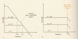
In practical VFB amps, open-loop gain is large at dc. But above a certain frequency, it rolls off at 6 dB/octave. At some frequency, the non-inverting open-loop gain is equal to the closed-loop gain nominally set by the ratio of feedback to input resistance. At that point, the actual gain of the closed-loop configuration is 0.707 times its dc value.
This frequency is designated the amplifier’s -3-dB bandwidth. In a VFB, the product of closed-loop gain and –3-dB bandwidth is called the gain-bandwidth product (GBWP). For a VFB amp, this is a constant for a certain range of frequencies (Fig. 4a). Designers must always trade off gain for bandwidth, or vice versa.
This isn’t true for CFB amps. There, closed-loop gain is again based on external component values, but it is largely independent of frequency (Fig. 4b). On the negative side, however, CFB datasheets limit the designer’s selection of feedback resistors.
In contrast, with a VFB op amp, the circuit designer has greater freedom in choosing the value of the feedback resistor (although higher resistance values may limit stability). VFBs also offer lower noise and better dc performance than CFB amps.
Generally, CFB amps are chosen when slew rate and exceptional low distortion are needed. VFB amps excel for dc applications, for applications requiring low input bias current or high input impedance, and where rail-to-rail performance is critical.
Amplifier Specs
Voltage-feedback op-amp datasheets specify five different gains: open-loop gain (AVOL), closed-loop gain, signal gain, noise gain, and loop gain. Without negative feedback, AVOL may be 160 dB or more. When an amplifier circuit’s feedback loop is closed, it exhibits less gain.
Loop gain is the difference between the open-loop and closed-loop gains or the total gain through the amplifier and back to the input via the feedback network. It comprises signal gain and noise gain. Signal gain is the gain experienced by an input signal. Noise gain reflects the input offset voltage and voltage noise of the op amp at the output. If both inputs of a differential-input amp are at 0 V, the output also should be at 0 V.
In reality, there’s always some voltage at the output, called the offset voltage, VOS. If the offset voltage at the output is divided by the noise gain of the circuit, the result is called the input offset voltage or input-referred offset voltage. VOS drifts with temperature, and TCVOS is the temperature coefficient of that drift.
Although ideal amplifiers have infinite input impedance, and, theoretically, no current flows into their input terminals, real amps that use bipolar junction transistors (BJTs) in the input stage require bias current (IB) for operation.
Total harmonic distortion (THD) reflects to the harmonically related components of the fundamental frequency caused by amplifier nonlinearity. Usually, only the second and third harmonics need to be considered. THD+N (THD plus noise) accounts for device noise.
THD and THD+N are both measurements of distortion generated by a single-tone sine-wave input. Intermodulation distortion (IMD) is a measurement of dynamic range produced by the interaction of two tones. Third-order intercept point (IP3) is a measure of the effects of third-order IMD.
The 1-dB compression point represents the level of input signal at which the output signal is compressed by 1 dB from an ideal input/output transfer function. This defines the end of an amp’s dynamic range. Signal-to-noise ratio (SNR) also defines the dynamic range. It is a measurement (in dB) from the maximum signal level to the RMS level of the noise floor.
In RF work, noise factor and noise figure are important specs. Noise factor relates the noise generated by the amplifier to the thermal noise of a 50-O resistor at room temperature. A noise factor of 2 means the amplifier is as noisy as a 50-O resistor. Noise figure is noise factor expressed in dB, i.e., 10 × log10 (noise factor).
Devices and Materials
For instrumentation applications, audio work, and RF up to VHF, conventional bipolars and field-effect transistors fabricated using conventional process technologies are the rule. The only difference between these processes and the ones used for mainstream digital ICs is that the analog parts tend to lag several generations behind in terms of design rules. That’s because it’s difficult to deal with system noise with amplifier input voltage swings below 3.5 V. On the other hand, at higher RF frequencies, exotic materials and advanced transistor architectures dominate. iSilicon-germanium (SiGe) is a silicon bipolar process technology in which the transistor bases are doped with germanium. To illustrate the advantages of SiGe in RF amplifiers, consider Maxim Integrated Products’ GST-3 process, a SiGe extension of its silicon GST-2 process. GST-3 offers an important decrease in transistor parasitic base resistance (RBB´) and a significant increase in ß.
In terms of noise figure, adding germanium to the p-silicon base of a transistor reduces the bandgap by 80 to 100 mV across the base, creating a strong electric field between the emitter and collector junctions. By rapidly sweeping electrons from the base into the collector, this electric field reduces the transit time (tB) required for carriers to cross the narrow base.
If all other factors are held constant, this reduced tB provides an approximate 30% increase in cutoff frequency (fT). Higher fT reduces high-frequency noise because the ß rolloff occurs at a higher frequency. For identical-area transistors, the SiGe device achieves a given fT with one-half to one-third the current required in the puresilicon device.
Maxim also notes that SiGe bipolars also require lower supply currents and provide higher linearity than conventional silicon transistors. Given high production volumes, SiGe devices are inexpensive and nearly as good as gallium arsenide (GaAs) in terms of noise figure and power. However, the higher the operating frequency, the lower the breakdown voltage, and hence the operating voltage.
The first microwave amplifiers were heterojunction bipolar transistor (HBT) metal epitaxial semiconductor field-effect transistors (MESFETs) and high electron mobility transistor (HEMT) MOSFETs, both built using GaAs process technologies. MESFETs are like junction FETs, but with a Schottky (metal-semiconductor) junction. HBTs use different semiconductor materials for the base and emitter. HEMTs are more common.
In a HEMT, the objective is to make electrons in the channel flow faster. In a doped channel, the doping atoms in the lattice impede the electrons. HEMTs rely on high-mobility electrons generated at the heterojunction. One side has a highly doped, wide-bandgap, n-type, donor-supply layer like aluminum gallium arsenide (AlGaAs). The other has a non-doped narrow- bandgap channel layer, such as GaAs.
The heterojunction between them forms a very thin quantum well in the conduction band on the GaAs side. The electrons can’t escape because of the well, but they travel very rapidly through it because there are no dopant atoms in the GaAs lattice. The layer they travel in is called an electron gas.
GaAs HEMTs are still made, but GaAs pseudomorphic high electron mobility transistor (pHEMT) and metamorphic high electron mobility transistor (mHEMT) devices are gaining lots of momentum. The terms pseudomorphic and metamorphic refer to the addition of indium phosphide (InP). The difference between the two lies deep in the semiconductor’s physics, but essentially, these techniques allow larger bandgap differences than conventional HEMTs. Ultimately, it gives them better performance.
Another alternative is to build indium-gallium- arsenide (InGaAs) HEMTs on an InP substrate. This results in very good high-frequency performance, but the technology hasn’t reached commercialization because InP wafers are extremely brittle.
Those GaAs MESFETs and HEMTs with very short gates suffer from high output conductance due to short-channel effects. In a silicon lateral double-diffused MOSFET (LDMOS), the short-channel effect isn’t present. With a positive potential on the gate, LDMOS devices create an inversion channel over the laterally diffused p-well at the silicon-oxide interface. The effective gate length may be shorter than the physical length of the gate electrode.
Other process steps extend RF performance and provide a high breakdown performance, allowing for operation at high supply voltages. LDMOS devices can also be made on silicon carbide.
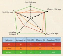
For RF amplifiers, plain old silicon still can challenge GaAs when the right understanding of transistor architecture is applied (see “HVVFETs—New In Town). In late April, a fabless company known as HVVi Semiconductors announced three new devices fabbed by ON Semiconductor in pure silicon using the company’s high-voltage vertical field-effect transistor (HVVFET) technology (Fig. 5).
About the Author
Comment About the Article
To join the conversation, and become an exclusive member of Electronic Design, create an account today!

Leaders relevant to this article: