Behind the ADC Veil: Demystifying Common DC Specifications (.PDF Download)

As its name implies, the function of an analog-to-digital converter (ADC) is to convert analog signals to digital representations for processing by a microcontroller (MCU), field-programmable gate array (FPGA), digital signal processor (DSP), or similar device.
In this article, we’ll review one of the most popular ADC architectures and how the dc specifications of a practical device differ from the ideal ADC model.
What Does an Ideal ADC Look Like?
Regardless of how it accomplishes the task, an ADC produces a digital output from an analog input signal, a process known as quantization. Quantization error results from this process since a digital signal can only have discrete values, whereas an analog signal may have any value within the dynamic range of the signal.
The quantization process leads to stair-step transfer function: Figure 1 shows this characteristic appearance in the transfer function of an ideal 4-bit ADC. This ADC divides the input voltage into 24, or 16, possible output codes, from 0000 to 1111.
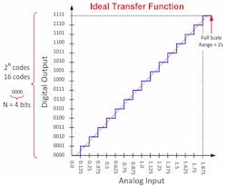
1. The transfer function of an ideal ADC. (Source: TI Precision Labs—ADCs: DC Specifications video)
In general, an n-bit ADC has 2n output codes. For a full-scale output of 2 V, each increase or decrease of 0.125 V (= 2/24) at the input (VIN) causes an increase or decrease of 1 count at the output. VIN = 0 gives an output of 0000; VIN = 0.125 V gives 0001, and so on.
