Clock Generators Bring Stability to Timing-Circuit Designs
Download this article in .PDF format
Clock speed is equivalent to data movement in applications that receive and process hundreds of megabytes of data each second. Applications involved in moving enormous volumes of data include cellular base stations and backhaul processors, medical imaging systems, and laboratory test instruments. These applications depend on receivers that can recognize multiple data threads within a single swollen stream. And they depend on precision timing circuits to transmit and extract the master clock signal.
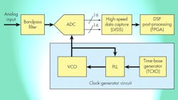
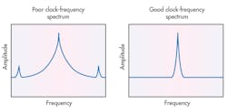
Such applications depend on complex but decipherable clock trees. Since the data transfers are triggered by clock edges—even at megahertz sampling rates—it’s crucial that each edge be distinguishable and readable. Clock spurs, clock jitter, and power-supply glitches can all be interpreted as false clock triggers and must be suppressed (Fig. 1).
It’s important, then, for engineers to understand the impact of timing-control components on the clock-and-data capture chain. The key elements in a timing chain—and some of their key specs—include:
• Precision oscillators, some with up to 1-GHz signal outputs, and with as little 0.1-ps jitter (or 90 fs). These enable system-wide improvements in bit error rate (BER), timing margins, and signal-to-noise ratio (SNR).
• Clock-generator packages integrate phase-locked loops (PLLs) and clock dividers in the same package. They help reduce the number of separate crystals and oscillators, and reduce bill-of-materials (BOM) costs. Their collective jitter specs are on the order of 150 fs.
• Clock distribution and fanout buffers include frequency dividers and delay lines, and output frequencies up to 3.1 GHz. The delay lines help synchronize multiple clock signals across a large circuit board.
• Clock-jitter cleaners include PLLs and clock redundancy circuits (send a sloppy signal in; get a clean one out). These are useful in noisy environments like automated factories.
• RF PLLs and frequency synthesizers include integrated PLLs and VCOs with low phase noise and spurs; integrated LDOs for very high supply noise immunity; and very low power consumption for mobile applications.
For the most part, this article will focus on “lower-frequency” circuits—those operating from 100 MHz to 1 GHz. A single gigahertz oscillator will go a long way to promote noise-free data streams; other components will stiffen jitter specs and phase margins. Additional components to consider include a crystal time-base reference, or transmit control crystal (a TCXO time base); a voltage-controlled oscillator (VCO); and a PLL.
The crystal oscillator generally serves as the time-base reference for the entire system. The time-base generator is often free of other electronics. If you imagine a piano tuning fork, you can visualize the musician pinging the fork to start it vibrating on a copy-able and repeatable musical note.
The crystal in a precision timing circuit is the equivalent of a mechanical tuning fork: a built-in oscillator pings the crystal, which is tuned to a specific copy-able and repeatable frequency. Ideally, the crystal and its oscillator are immune to atmospheric changes such as temperature drifts and humidity. Consequently, crystal-oscillator drift is generally within ±50 ppm over time and temperature.
The remaining parts of the timing-control system include a VCO whose frequency output is a function of the input voltage it receives (recognizing the importance of low-noise power supplies). A separate PLL compares the output of the VCO to the frequency set by the time-base generator, and latches to the chosen frequency.
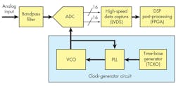
Each component in the timing chain must be carefully selected and embedded to avoid adding frequency jitter—and spurious edges—to the clock signal. The roles they play can be visualized, for example, on the front end of a high-speed data-capture circuit (Fig. 2).
Choosing a VCO: Know the Contribution to Jitter
A major factor regarding the timing of the clock-generator circuit is the choice of VCO. Inside the clock generator, a comparator circuit compares the input frequency (from the time-base generator) and the VCO output frequency. It produces a dc voltage that’s proportional to the phase difference between the two frequencies.
For gigahertz sampling circuits, the VCO should be able to generate oscillator frequencies up to 1 GHz. But the task of choosing a VCO for high-speed data converters is more than a matter of clock frequency. The contribution to jitter must be carefully weighed.
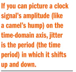
Phase noise and jitter actually describe the quality of an oscillator. Jitter (as we’ve said) is a time-domain representation of timing accuracy; phase noise is actually the frequency-domain representation of the same signal. It tells you what kind of noise will be in the spectrum surrounding the signal carrier frequency.
Equipment measuring jitter in the time domain (long persistence oscilloscopes, for example) will help you visualize the effects of jitter on high-speed serial links in real time. Frequency-domain equipment, such as a phase-noise analyzer, on the other hand, measures the RMS power of a signal in a chosen frequency band.
Jitter generated by a clock source can cause the analog-to-digital converters (ADCs) to trigger falsely. Uncertainty in sampling time equates to uncertainty in signal amplitude (you’re likely reading an amplitude peak that shouldn’t be there). This results in false sampling of the analog input amplitude, and degrades the SNR of the ADC.
Low-Voltage Differential Signaling
Sampling signals at high frequencies (1 Gsample/s and above) means that the digital output data produced by the conversion—multi-megabytes—must be stored (or transferred somewhere) at very fast data rates. When your ADC is handling gigahertz data streams (effectively a billion conversions per second), you need to maintain signal integrity among the digital components and affect a clean data transfer for each clock cycle. Low-voltage differential signaling (LVDS) has become the choice for moving high-speed data from ADCs on the front end of a data-capture system to the back end where the data is processed.
LVDS signaling, when used with field-programmable gate arrays (FPGAs), enables high data rates with relatively low power consumption in applications like backhaul processing and medical imaging (ultrasound scanning). Only two wires are required for each discrete signal carried.
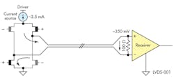
As defined by the LVDS standard, the differential signal lines use 100-Ω terminations. A signal voltage of 350 mV generated across this resistor will pull a 3.5-mA current from the transmitter source. The transmitter circuit provides enough voltage for the receiving circuit to detect (Fig. 3).
Low-voltage differential signaling is ideal for telecommunications and data-communications applications like switches, hubs, and routers. It’s also useful for computing applications such as digital copiers, processor interfaces, imaging displays, audio and video digital signal processing, and MPEG stream processing.
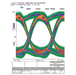
The Eye Diagram
Ideally, you want an open eye pattern on the captured data. An “eye diagram” is a visual representation of the jitter and clock driver quality of a received LVDS output signal. The diagram is obtained by sending pseudorandom data over the LVDS channel and using a sampling oscilloscope to perform a “persistence” measurement. The signal transitions are captured and plotted over time.
A zero jitter measurement indicates that the signal transition occurs at exactly the same point in time for each transition (it doesn't shift up and down on the time axis). Transitions in the eye-pattern diagram—shifts up and down over a wide slice on the time axis—are the results of high jitter. They suggest the transmitted signals aren't transitioning consistently at the required time. A small eye width implies a large-variation signal-transition time.
Horizontal eye closure is thus due to jitter (frequency shifts on the transmitted data, measured in picoseconds), while vertical eye closure is due to signal (amplitude) attenuation or noise. Therefore, a larger “eye” indicates a better quality driver (for example, the eye diagram for an LVDS receiver is shown in Fig. 4).
Simulating Clock-Tree Performance
Many leading analog manufacturers offer simulators and performance analyzers for clock-tree design. These systems allow engineers to visualize the performance of clocking systems using discrete crystals and clock oscillators, and are often linked to the specific timing-control components supplied by the semiconductor manufacturer.
Using discrete crystals and oscillators in a clock tree will likely point to readily available components (like crystal oscillators). These can often lead to an increase in bill-of-materials (BOM) cost, and result in less-than-optimum performance of the timing-control system. Ideally you want to simulate performance with models of advanced components—with built-in PLLs and selectable delay lines—and not just the crystal oscillators.
In addition to recommending optimized clock-tree solutions, the most modern simulation tools will enable advanced PLL designs by simulating phase noise (as well as the impact of jitter). With the best simulators, you can even enter custom phase-noise profiles for external references such as crystal oscillators (XOs), voltage-controlled crystal oscillators (VCXOs), and silicon-based voltage-controlled oscillators (VCOs). Accurate modeling of external reference sources improves the accuracy of the clocking system beyond the phase-noise and jitter specifications.

About the Author
Comment About the Article
To join the conversation, and become an exclusive member of Electronic Design, create an account today!

Leaders relevant to this article: