Enhance Synchronous-Rectification Control In Flyback Converters
By Mario Battello, Marco Soldano, and Maurizio Salato, International Rectifier
The transition from diodes to synchronous-rectification (SR) MOSFETs in secondary circuits of flyback converters increases with each new generation of MOSFETs, improving performance at little or no cost penalty. SR MOSFETs can be more efficient than diodes, allowing lower operating temperatures and smaller heat sinks, or no heat sinks at all. However, they require a control circuit to manage their switching behavior in order to emulate a diode. The usual synchronous rectifier control method in today's commercial power supplies involves deriving the logic signal for the controller from the secondary of a current transformer. There is a better way, though.
Flyback History
Traditionally, flyback converters were well suited for applications requiring power levels less than 150 W. Their major appeal was simplicity and low cost. Beyond 150 W, and certainly at power levels of 200 W and beyond, the half-bridge- and forward-converter were the standard topologies. The major problem with flybacks, whether they were implemented with diodes or SR MOSFETs, was semiconductor conduction losses.
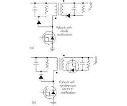
As with all isolating power-converter topologies, flybacks employ a transformer on the secondary, on which resides a rectifier. The simplest configuration uses a half-wave rectifier diode on either the high or low side (Fig. 1a). Synchronous rectification combines a MOSFET with some kind of control for turning the device on or off so that it emulates the diode commutation of the ac from the transformer. The synchronous approach provides greater efficiency, albeit with a corresponding tradeoff in complexity and cost (Fig. 1b).
1. Basic topologies for flyback secondary rectification use a diode (a) or an SR MOSFET (b).
What kind of losses are we talking about? For a diode, the forward-conduction power loss is simply the product of the forward voltage and current. For a MOSFET, it's I2 RDS(ON). When a diode has a standard 0.6-V VF, a 4-A current turns 2.4 W into heat. And, if a MOSFET's RDS(ON) = 10 mΩ , the loss at 4 A is 0.16 W (see the table).
At 4 A, the MOSFET dissipates 93% less power, leading to a lower junction and case temperature, meaning that it requires either a smaller heat sink or no heat sink at all. Theoretically, for the diode and MOSFET characteristics in the example, power-loss parity doesn't occur until current reaches 60 A. In practice, long before you reach power-loss parity in a real circuit, you would choose a MOSFET with a lower RDS(ON), parallel a pair of devices, or choose a different architecture.
Synchronous Rectifier-MOSFET Control
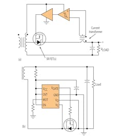
Though SR brings significant efficiency and thermal-management advantages over diode rectification, those advantages don't come for free: You need a gate-control signal to properly operate the FET. A popular approach to gate control uses a current transformer, a comparator, and a gate-driver stage. A simplified schematic of this arrangement appears in Figure 2a.
The current transformer senses the secondary current, imposing scaled copy on its load impedance, which results in a voltage proportional to the current, preserving the polarity information. The comparator detects this voltage and turns on the MOSFET through the driver when the secondary current conducts in the forward direction.
Though conceptually simple, the current-transformer-based SR control presents a few challenges. The first derives from the fact that transformers, be they voltage or current transformers, are ac-coupled devices. The current transformer's secondary signal, therefore, is bipolar, so the downstream signal processing must take that into consideration. This complicates the power-transformer design by an additional secondary-winding segment and adds a rectifier and filter to strike a second rail for the comparator and driver.
2. Here, an SR flyback-converter output stage is based on a current trasformer (a) and an IC that implements a new alternative control method (b).
The second challenge is that in its full implementation, this circuit requires as many as 15 components. These components, and their associated routing, require a large pc-board area comparable to that of a feedback control circuit.
A third challenge relates to timing. As an analog signal processor, the current-transformer-based SR control?s performance is subject to the variations of many of its components over their operating temperature range, as well as to the current transformer's parametric distribution over a production run.
Delays through the current transformer and further delays due to parasitic capacitances at the comparator inputs prevent this circuit from responding to the current-polarity change as quickly as the simplified schematic might suggest. A measurable lag occurs, therefore, between the current's zero crossing and the time when the driver shuts off the switch. During this interval, reverse current steals charge from the bus capacitor, reducing efficiency and increasing output ripple. Indeed any secondary circuit that allows reactive energy to slosh back and forth between the transformer and bus capacitor suffers in this way, so tight timing to the current's zero crossing is critical to a highly efficient secondary circuit.
Finally, commercial IC implementations use phase-locked-loop (PLL)-based circuits, the major limitation of which appears to be in transient response due to the primary side's variable-frequency control.
An alternative to current-transformer-based designs is to use a pair of comparators that differentially sense the MOSFET's drain-to-source voltage to determine the polarity and level of the current. This dc-coupled measurement can drive logic that turns the power device on and off near the zero-current transitions. No PLLs or external timing sources are necessary, and the control circuit operates on a unipolar supply (Fig. 2b).
Using the power MOSFET's on-resistance as a measurement shunt, the input comparators sense the rectifier current. Internal blanking logic prevents spurious transitions and guarantees proper operation in continuous-conduction mode (CCM), discontinuous-conduction mode (DCM), and critical conduction mode (CrCM) (see "Modes of Conduction"). This flexibility means that the secondary-circuit control method doesn?t constrain your choice of primary-circuit operation mode.
Modes of operation for a flyback circuit differ mainly for the turn-off phase of the SR switch. On the other hand, the turn-on phase of the secondary switch, which corresponds to the turn-off phase of the primary-side switch, is identical. This makes possible a variety of converter control schemes, including fixed-frequency, quasiresonant; variable-frequency; and fully resonant, actively clamped converters with switching frequencies as high as 500 kHz.
Turn-On Phase
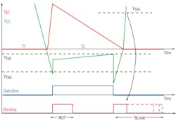
At the start of the SR FET's conduction phase, current begins to flow through its body diode, generating a negative drain-to-source voltage across it. The body diode maintains a higher voltage drop than that of the device's drain-source channel. Therefore, it triggers turn-on threshold voltage VTH2 (Fig. 3).
3. Comparators measuring VDS across the secondary SR FET quickly trigger the gate drive on when current through the FET’s body diode indicates forward conduction. They shut off the gate drive as the secondary current approaches its zero crossing. Minimum on time (MOT) and a blanking interval (tBLANK) prevent spurious operation resulting from ringing on the front end, or the body diode conduction on the trailing end, of the conduction cycle. tBLANK
At that point, the control logic drives the MOSFET's gate on, which in turn causes the conduction voltage (VDS) to drop. Some ringing usually accompanies that voltage drop, and the ringing can trigger the input comparator to turn off. This can be dealt with by using an externally programmable minimum on-time (MOT) blanking period that maintains the power MOSFET in the on state for a minimum interval. The programmable MOT also limits the SR MOSFET's minimum duty cycle and, as a consequence, the maximum duty cycle of the primary-side switch.
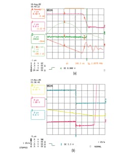
The synchronous MOSFET's turns-on and -off behavior closely emulates the diode's function, thanks to the use of the same device as the sensing element. This approach obtains the highest possible performance for a given switch, often enabling the use of smaller switches. The control resolution of a discrete implementation is often insufficient to measure the current waveform close to its zero crossing, allowing the current to invert before switching off (Fig. 4a).
4. Shown are SR turn-off waveforms for a commercial current-transformer-based control (Ch2: VGS; Ch4: VDS; ChA: ID) (a) and the IR1167 (Ch1: ID; Ch2: VDS; Ch3:VGS) (b).
DCM/CrCM Turn-Off Phase
Once the SR MOSFET turns on, it remains on until the rectified current decays to the level at which the drain-to-source voltage ( VDS) crosses the turn-off threshold voltage VTH1. How this action takes place depends on the mode of operation.
In DCM, the current crosses the threshold with a low di/dt. Once the current crosses the threshold, it once again flows through the body diode, causing a negative step in VDS . Depending on the amount of residual current, VDS might again trigger the turn-on threshold. To prevent this, an internally set blanking interval (tBLANK) causes the controller to ignore this VTH2 crossing. As soon as VDS crosses positive threshold VTH3, this blanking time terminates, and the controller is ready for the next conduction cycle.
Control Method Comparison
Although implementing this scheme using discrete components would be challenging, and would involve a high parts count and considerable board space, the concept is attractive if implemented as an IC. One particular single-chip instantiation, the IR1167, needs only three external components. The chip, plus a decoupling capacitor, a gate resistor, and a programming resistor, fits into less than 160 mm2 (0.25 in.2).
For zero-voltage switching (ZVS), the primary is necessary. Otherwise, any reactive power flow between the secondary- and the primary-converter stages reduces overall system efficiency. Traditional transformer sensing requires high current, which causes additional conduction losses. These losses at least partially erode the advantage of primary-ZVS operation. The new control method's gate turn-off falls close to the secondary current's zero crossing, but always on a negative threshold. Therefore, this approach eliminates reactive power flow between the output capacitors and the transformer (Fig. 4b).
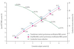
This FET-voltage-based approach has only negative drain-to-source-voltage thresholds. As a result, SR drain-to-source current can't flow through the device under any condition. This fact, in turn, reduces the overall power flow and, thereby, losses in the primary circuitry, including switches and magnetics. Figure 5 shows the impact on secondary-current rms value and the consequent reduction in conduction losses on a 120-W, 19-V laptop adapter.
The IR1167 also allows CCM operation without further circuit modification. Although traditional current-transformer-based designs can work in DCM or CrCM, they can?t efficiently work in CCM. The new control method allows operation in all modes, providing the best efficiency and cost-effectiveness.
5. At low idle or standby currents, the IR1167’s SR FET turn-off behavior reduces converter losses in a 19-V 120-W laptop ac adapter to more than 23% at 1 A and 8% at 6 A.
The power necessary for controller operation is generally lower than that for designs using discrete parts, thanks to the device's gate-voltage-level clamp and high integration. Independent of the VCC supply, the gate charges to 10.7 V. As the trend toward greater switching frequencies continues, particularly with the increasing adoption of resonant controllers, and as paralleling devices boost the gate charge, gate-switching losses account for an increasingly significant amount of power.
The IR1167's gate clamp can reduce those losses. With a 1-nC gate charge, the effect is small ? even at relatively high frequencies. However, at 15 and 30 nC, this gate-drive modification saves in excess of 0.7 and 1.8 W, respectively, of switching power at 500 kHz. The power losses in synchronous FETs are often less than 1 W; this simple reduction in gate-drive level can easily save a comparable amount of power.
The IC also has a sleep mode, which further reduces current consumption. All of these factors help meet the upcoming stringent standards on power consumption under standby, extremely light load conditions.
Experimental Results
The following comparison characterizes two commercially available universal-input supplies using flyback topology before and after implementation of the new control technique on the secondary side. The comparison measures efficiency and thermal performance in a thermal chamber at a 45ºC ambient temperature.
24-V, 150-W LCD TV open-frame power supply operating at full load (6.5 A) at 45°C ambient: This design provides an active front-end power-factor corrector with two bus voltage-levels, depending on the mains. The secondary circuit's synchronous rectifiers are two 10.5- mΩ MOSFETs in TO-220 packages. The SR drive circuit is a discrete voltage-based controller. The system retrofit consists only of an IR1167 controller, which replaces the original discrete voltage-based contoller; the SR devices and their associated thermal system remain unchanged.
The retrofit improved the supply's overall efficiency by between 0.6 and 0.9% over the input voltage range (100 to 240 V) while reducing the SR FET's tab temperature by between 15.9 and 17 ° C over the same voltage range.
19-V, 90-W laptop adapter operating at full load (4.62 A) at 45°C ambient: This design provides an active-front-end boost-follower power-factor corrector. The secondary circuit's rectifiers are two 100-V, 30-A, Schottky diodes in TO-220 packages. The system retrofit consists of an IR1167 and two 100-V, 18- mΩ IRF7853 MOSFETs in SO-8 packages.
The retrofit improved the laptop adapter's overall efficiency by between 1.0 and 1.3% over the test input voltage range (120 to 240V), while reducing the SR FET's case temperature by between 6.1 and 8.2 ° C over the same voltage range.
As these efficiency and thermal data indicate, standard flyback-system designs can easily implement SR functions or enhance the efficiency of their current implementations.

