Download this article in .PDF format
It comes as no surprise that a large-scale data center, enterprise server, or telecom switching station uses a lot of power. Data-center electricity consumption in the U.S. is projected to increase to roughly 140 billion kilowatt-hours annually by 2020. This usage is equivalent to the output of 50 power plants; the total data-center electricity bill is around $13 billion annually.
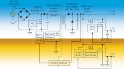
Figure 1 shows a typical power-conversion architecture for a data-center server farm. Although most of the stages are extremely efficient, the overall result is an efficiency of only around 67%. The last two dc-dc stages are not only the least efficient, they’re also located in the most space-constrained environment: the server rack or motherboard. Since the wasted energy is dissipated as heat, decreased efficiency here leads directly to increased cooling costs. Thus, designers always strive to boost the performance of these stages.
Many designers of such systems are standardizing on a 48-V power-distribution architecture combined with point-of-load (POL) dc-dc converters. A higher bus voltage reduces the current for a given power level, which minimizes distribution losses. Google, for example, has proposed such a rack architecture to the Open Compute Project, an industry consortium focused on developing energy-efficient data centers.
At the dc-dc stages, this is driving the adoption of new semiconductor materials and high-efficiency POL designs that can convert 48 V to 1 V in a single stage.
The Case for Gallium Nitride
For many years, silicon has been at the heart of the vast majority of semiconductor devices. Now, however, gallium nitride (GaN) is replacing silicon as the material of choice for power transistors in industrial automation, motor drivers, high-frequency dc-dc conversion, and similar applications.
Why use GaN? It’s one of a class of wide-bandgap (WBG) semiconductors that have superior performance to silicon in power applications. GaN’s bandgap energy is 3.4 eV, compared to 1.1 eV for silicon. The higher energy gives GaN power transistors a number of advantages, including:
• Lower gate capacitance and output capacitance for higher switching frequency with lower switching losses.
• Higher efficiency, resulting in lower conduction and switching losses, and low or zero reverse recovery losses.
• A smaller footprint for higher-power-density designs.
• Lower RDS(on) for higher current operation.
There are other WBG semiconductors, notably silicon carbide (SiC), with a bandgap energy of 3.3 eV. Still, GaN is expected to dominate in high-performance power applications up to about 50 A and 200 V.
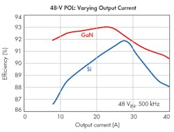
In a 48-V POL dc-dc converter, switching from Si to GaN results in an efficiency improvement across the board (Fig. 2).
Combine Driver and GaN for Best Performance
Although GaN transistors switch much faster than silicon MOSFETs and can achieve lower switching losses, it’s important that the rest of the design helps make the most of these advantages.
GaN devices are typically packaged separately from their drivers because they use different process technologies. Each package can introduce additional parasitic inductance into the circuit from internal bond wires or printed-circuit-board (PCB) interconnects, and this can limit GaN switching performance at high slew rates. Integrating the GaN FET and driver into the same package reduces parasitics and optimizes switching performance.
A single package also makes it easier to include protection features. Overcurrent-protection circuits, for example, require low-inductance connections between the GaN device and its driver. Extra inductance can cause ringing and requires a long blanking time to keep the current protection from misfiring. Integrating the driver minimizes the inductance between the sensing circuit and the GaN FET so that the current-protection circuit can react as quickly as possible.
Since the package lead frame is an excellent heat conductor, the temperatures of the driver and GaN FET can track each other closely. Thermal sensing and overtemperature-protection circuits can then be included on the driver chip to protect the FET.
Architectural Benefits of GaN Devices
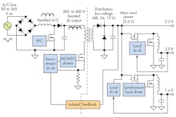
Using a GaN power stage has architectural advantages, too. Figure 3 shows the ac-dc and dc-dc stages in the power-conversion chain discussed earlier. The 48-V dc or 12-V dc bus voltage on the secondary side of the isolation transformer is stepped down to an intermediate 3.3 V; then one or more buck converters generate the voltages needed for processors and other components.
A GaN device allows the design of a single-stage, high-efficiency, 48-V-to-1-V dc-dc converter. The elimination of the intermediate stage saves cost and reduces size at the board level; at the room level, it also reduces cooling costs.
GaN DC-DC Converter Topologies
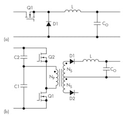
Several different dc-dc converter topologies can be used to convert 48 V to 1 V, each coming with advantages and disadvantages. The buck converter is perhaps the simplest and lowest cost, but has lower efficiency. The transformer-based half-bridge topology, on the other hand, is considerably more complicated and offers higher efficiency at a higher cost.
The half-bridge topology efficiently supports a high step-down ratio while providing fast transient response and significant output current courtesy of the full-wave rectifier on the secondary side of the transformer. Let’s look at a half-bridge design example in more detail.
Application Example
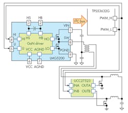
Figure 5 shows the block diagram of an efficient 48-V/1-V POL converter design using the LMG5200 80-V, 10-A GaN half-bridge power stage, and the TPS53632G half-bridge POL controller.
The LMG5200 provides the primary-side FETs Q1 and Q2 in Fig. 4b. It integrates two 18-mΩ GaN FETs and their driver into a single device. To minimize parasitic inductances, all three devices are mounted in a nine-pin QFN package that contains no bond wires.
The TPS53632G controller uses a D-CAP+ hysteretic control architecture and features Valley Current Mode with adjustable ON time control, adjustable slew rate, and fast transient response. The part can switch up to 1 MHz when paired with a suitable GaN power stage. An I2C Rev 3.0 interface enables output voltage control and feeds back current-monitoring information.
The secondary side includes a current-doubler rectifier, a refinement of the full-wave rectifier shown in Fig. 4b. In this configuration, the transformer secondary isn’t center-tapped; instead, there are two inductors, each carrying half of the dc output current. This arrangement adds complexity, but simplifies the power transformer design, dissipates less power, and requires smaller magnetic components.
To further increase efficiency and lower power dissipation, a UCC27523 dual low-side MOSFET driver and two EPC2023 GaN FETs replace the diodes to add synchronous rectification to the current-doubler circuit. The TPS53632 provides the drive signals for the UCC27523.
Although this design is non-isolated, an isolated version can be implemented by adding a digital isolator such as the ISO7820 between the TPS53632 and the primary-side devices.
The LMG5200POLEVM-10A evaluation module (EVM) is available to evaluate this design. The user manual includes the complete schematic, which supports input voltages from 36 to 75 V and output voltages from 0.5 to 2.5V.
Layout Guidelines
As discussed earlier, it’s important to optimize all aspects of the design to take full advantage of GaN technology, and no more so than in the PCB layout.
Reducing parasitic capacitance is particularly critical. For example, it’s vital to minimize any capacitance from the switching node to ground or VIN. Any parasitic capacitance must be charged during FET turn-on, which increases switching losses. It’s also important to pay attention to interlayer capacitance in multilayer boards. Even heat sinks with insulated thermal interfaces can add parasitic capacitance.
Interference is another issue to be managed. High-power GaN switching can interfere with low-level logic devices, and poor layout can cause a range of undesirable effects ranging from inadvertent turn-ons to shoot-throughs and false triggers.
GaN layout guidelines are covered in more detail in TI’s application note SNOA946, which discusses another half-bridge GaN design, this one using the LMG3410 600-V, 12-A Smart GaN power stage.
Conclusion
GaN transistors offer key advantages to designers of low-voltage, high-current POL converters for telecom and server applications. To make the most of their performance, though, it’s necessary to pay attention to some key design guidelines.
TI has a range of GaN solutions, evaluation boards, application notes, and tools that cover these areas and help engineers develop a successful design.
