Inkjet-Printed Graphene Plus Laser Yields Washable Electronics

When Professors Sir Andre Geim and Sir Kostya Novoselov of the University of Manchester (UK) discovered and isolated a single atomic layer of carbon for the first time—now known as graphene—there was both praise and concern. Some comments were similar to those which, decades before, accompanied the first demonstration of the optical laser, heralding it as “a solution looking for problems to solve.” (Note that the professors received the Nobel Prize in Physics in 2010, in recognition of their work.)
Of course, we know how the story of the laser’s applications turned out with its truly countless uses, many of which were literally unimaginable at the time. Graphene is tracking along a similar trajectory with applications in high-performance batteries and supercapacitors, advanced high-strength and lightweight materials, materials having extremely high thermal conductivity, plus many more.
Among the latest developments is the use of graphene as the basis for washable electronics, from a research team led by Iowa State University. By combining graphene and sophisticated laser-based processing, they have developed circuits that are low-cost, flexible, highly conductive, and water-repellent.
“We’re taking low-cost, inkjet-printed graphene and tuning it with a laser to make functional materials,” said Jonathan Claussen, an assistant professor of mechanical engineering and an associate at the U.S. Department of Energy’s Ames Laboratory, as well as the corresponding author of the paper published in the journal Nanoscale “Superhydrophobic inkjet printed flexible graphene circuits via direct-pulsed laser writing” (with additional modeling, simulation, and supplemental information here). The material and resultant circuitry could be useful for a wide range of applications such as self-cleaning, wearable, or even washable electronics, they claim.
The process begins with an inkjet printer (another mass-market product finding all sorts of fascinating, unforeseen applications such as 3D printing), where the “ink” consists of flakes of graphene, an excellent electrical conductor that’s also strong, stable, and biocompatible. Unfortunately, the printed flakes aren’t highly conductive and have to be processed to remove non-conductive binders and weld the flakes together, thus boosting conductivity and making them useful for electronics or sensors. By applying a technique called direct-pulsed laser writing (DPLW), the team was able to adjust and fine-tune the water-retaining/repelling characteristics and electrical conductivity of the inkjet-printed graphene (IPG).
Wash and No Wear
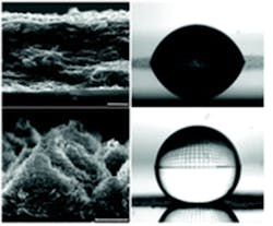
The graphene surface pattern (left) and wettability contact angle (right), shown before (top pair) and after (bottom pair) the direct-pulsed laser writing procedure. (Source: Iowa State University)
The DPLW rapid-pulse laser process treats the graphene without damaging the printing surface—even if paper or ultrathin polymers—and transforms graphene-printed circuits that can hold water droplets (hydrophilic) into circuits that repel water (superhydrophobic). Their experimental results indicate that the DPLW process can convert the IPG surface wettability from one that’s initially hydrophilic (contact angle CA of about 7.7°) and electrically resistive (sheet resistance ∼21 MΩ per square) to one that’s superhydrophobic (CA ∼157.2°) and electrically conductive (sheet resistance ∼1.1 kΩ per square) (see figure).
“We’re micro-patterning the surface of the inkjet-printed graphene,” said Claussen. “The laser aligns the graphene flakes vertically—like little pyramids stacking up. And that’s what induces the hydrophobicity.”
The energy density of the laser processing can be adjusted to tune the degree of hydrophobicity and conductivity of the printed graphene circuits. (Note that DPLW is another one of those fascinating technologies having widespread, disparate applications including welding tiny materials, “drilling” precision holes without burrs or workpiece distortion, microsmoothing and super-polishing finished surfaces, and printing identification legends on tiny devices.)
The studies are supported by the National Science Foundation, the U.S. Department of Agriculture’s National Institute of Food and Agriculture, the Roy J. Carver Charitable Trust, and Iowa State’s College of Engineering and department of mechanical engineering. The Iowa State University Research Foundation is hoping to patent the technology, and has also optioned it to NanoSpy Inc. ( an Ames-based startup) for possible commercialization.
Reference

About the Author

Bill Schweber
Contributing Editor
Bill Schweber is an electronics engineer who has written three textbooks on electronic communications systems, as well as hundreds of technical articles, opinion columns, and product features. In past roles, he worked as a technical website manager for multiple topic-specific sites for EE Times, as well as both the Executive Editor and Analog Editor at EDN.
At Analog Devices Inc., Bill was in marketing communications (public relations). As a result, he has been on both sides of the technical PR function, presenting company products, stories, and messages to the media and also as the recipient of these.
Prior to the MarCom role at Analog, Bill was associate editor of their respected technical journal and worked in their product marketing and applications engineering groups. Before those roles, he was at Instron Corp., doing hands-on analog- and power-circuit design and systems integration for materials-testing machine controls.
Bill has an MSEE (Univ. of Mass) and BSEE (Columbia Univ.), is a Registered Professional Engineer, and holds an Advanced Class amateur radio license. He has also planned, written, and presented online courses on a variety of engineering topics, including MOSFET basics, ADC selection, and driving LEDs.
Comment About the Article
To join the conversation, and become an exclusive member of Electronic Design, create an account today!

Leaders relevant to this article: