The selection criteria for analog-to-digital converters (ADCs) and digital-to-analog converters (DACs) can seem overwhelming at first. There is a broad array of analog requirements for sample rate, resolution, usable bandwidth, power consumption, spurious free dynamic range (SFDR), and other performance metrics that will dictate how well a system will behave.
Related Articles
- Synchronize Multiple ADCs With JESD204B
- Slay Your System Dragons With JESD204B
- Kickstart Your System Designs With JESD204B
Many converters today sport the latest high-speed serialization/deserialization (SERDES) interface, JESD204B. Now, their digital portion also becomes part of the selection criteria when they’re connected to an FPGA. JESD204B converters, then, must be prototyped with a capable FPGA. This can be unchartered territory for some designers, as there is sparse industry experience with this new interface.
We often hear questions from system designers about how to get from the converter datasheet to a complete system prototype with JESD204B that works as expected. Designers can take advantage of several common practices to launch a functioning converter system with JESD204B and an FPGA.
This file type includes high resolution graphics and schematics when applicable.
The analog input configuration for the converter evaluation board is optimized to achieve full datasheet performance. Typically, the board will demonstrate the full bandwidth of the converter. Often, if the full bandwidth is desired, a system designer can use most of the front-end layout for the application, with only slight modifications to meet its unique specifications. But if only a selective pass-band portion of the full spectrum is needed, a system designer will need to design a custom filter to meet the need of their system.
Evaluate With An FPGA Using FMC
The first step in prototyping a JESD204B converter is to choose from the short list of converters that meet the analog performance metrics of the system. Vendors typically offer a device evaluation board for system designers to wring out the component operation. To capture data from an ADC or send data to a DAC, a data capture or source solution is also needed.
Typically, this is done in one of two ways. First, a dedicated FPGA can be populated on the converter board for a one-board solution. Or, a more popular method is to separate the FPGA on a dedicated capture or memory board that interfaces to the converter board with a high-speed connector. A popular industry standard connector now being used is the FPGA Mezzanine Connector (FMC).
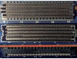
The FMC interface is a surface-mount component that provides an industry-standard pin designation for the high-speed I/O, control pins, and power supply, mapped across the connector to and from an FPGA. The bandwidth of the connector is sufficient to handle up to 10 receive and 10 transmit lanes of the highest-speed JESD204B data rates of 12.5 Gbits/s. The standard format and pin designation of the FMC makes it easy for plug and play use between FPGA evaluation kits and interfacing components such as ADCs and DACs (Fig. 1).
Choose Firmware And IP
A converter vendor will need to have some FPGA JESD204B firmware available on the evaluation board so a DAC can be sourced with data or an ADC’s data can be captured. However, this may only be prototype firmware that is specifically developed for evaluation and not suitable for an end system.
The leading FPGA vendors, Altera and Xilinx, both offer JESD204B intellectual property (IP) cores for their respective FPGA families that cover nearly all of the cases needed to support data converters with this interface, up to the maximum lane rate of 12.5 Gbits/s. The IP can be configured for the specific system application. In addition, behavioral models are provided to complete the simulation. While the evaluation platform may use a capable FPGA model, this may not be the same FPGA that will suit the end system. The number of converters, links, lanes, and processing capabilities must be determined to choose the right FPGA.
A rapid prototyping version of the converter evaluation board may be available, in which case it can be used with an open market FPGA kit. For those kits that provide two FMC connectors, a dual converter system can be demonstrated for synchronous processing using the hooks included in the JESD204B subclass 1 interface. This subclass provides for a system reference signal to align data within the FPGA from multiple converters that could each have a different latency.
Model
To simulate the performance of the JESD204B link in the design phase of a system, a model can be used that emulates the operation of each physical-layer (PHY) component on the link. For a JESD204B link, the primary components are the transmitter, printed-circuit board (PCB), optional connector or backplane, and receiver. Since the transmitter and receiver are the only active components of the link, they can also provide channel compensation to improve the signal quality and reduce the long-term bit-error rate.
In a typical JESD204B interface, a passive PCB channel will act as a low-pass filter in the system due to the capacitive effective of the PCB traces with the dielectric material of the board. Additionally, any cable, backplane, or connector within the spatial link also will be part of the channel. Active transmitter pre-emphasis and de-emphasis from an ADC output coupled with receiver equalization (EQ) on a DAC input can effectively boost the high-frequency content for the total system as seen at the end receiver.
If the active channel compensation settings are dialed correctly for the particular system, the result is a nearly flat frequency response through the transmission link. Ideally, all these methods can be modeled, using a signal integrity (SI) computer automated design (CAD) simulation, to predict the bit-error margin and performance over the link. The known properties of the channel such as PCB length, connector properties, and dielectric material constant within the transmission line can be optimally modeled against the settings of the transmitter and receiver channel compensation.
The model for all the active components is commonly known as an IBIS-AMI (I/O Buffer Information Specification – Algorithmic Modeling Interface). The IBIS-AMI model should be available from both your JESD204B converter and FPGA vendors. The passive components of the PCB traces and connectors also can be modeled based on the trace length, width, spacing, impedance, and dielectric material. The algorithmic portion encompasses the digital behavior of the JESD204B including expected jitter, timing delays, and any digital channel compensation. The analog model exhibits the rise and fall slew rates, bandwidth, and swing amplitude of the signal on the pin (Fig. 2).
Simulate
Several open market SI tools can run a complete system simulation using the IBIS-AMI models from each component of the link. The active component models provide register settings to alter the active channel compensation on the transmitter and receiver. The channel compensation parameters are variables that can be changed within the IBIS-AMI model to easily adapt and re-run a simulation.
If marginal or failing results are seen from simulation of the serial interface, the system designer may need to alter portions of the design to meet performance. Some potential changes could include shortening or modifying the PCB trace widths and lengths for optimum bandwidth and matched impedance, using a lower dielectric PCB material, choosing connectors or backplanes with lower insertion loss, or increasing the active channel compensation parameters on the transmitter and receiver. Alternatively, a matrix simulation sweep against all possible options can be done to identify the optimum best case solution.
System Evaluation
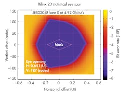
In the final system, an internal probing tool can be used to visualize the recovered eye diagram of the serial data seen after the FPGA receiver’s adaptive gain control and equalizer. Analog Devices and Xilinx have co-developed a tool called EyeScan to be able to see this information. While not an exact measured signal, it is based on a persistence compilation using thousands of comparison points. An overlay of a fine sweep of the FPGA internal comparator voltage, or codes, on the y-axis versus small time delays in relative unit intervals (UI) of a period along the x-axis creates the image (Fig. 3).
The output can be seen in a software graphical rendering of the data sweep involving both of these variables. Over a large population of bits, the EyeScan can show signal density in concentric circles around the eye that can be recovered for varying contours of bit-error rates, relative to the defined keep-out mask. This is a cost-effective solution for final system validation that does not disrupt the signal with external probes. It also allows the benefit of seeing past the last PHY component of the SERDES link, the receiver’s internal equalizer.
With this system tool, the pre-emphasis from the transmitter or the equalization gain from the receiver can be finely tuned to meet the needs of the particular application. The recovered eye diagram can be opened to its maximum or closed down depending upon the channel compensation settings. Increased power consumption on either end of the link typically will be the main tradeoff for better eye diagram performance. The results should match those seen in the IBIS-AMI simulation model of the same parameters.
The converter vendor will provide a unique set of evaluation software interface tools to control the converter and process the data to and from the device. This will allow system designers to program all the register options to fully configure the converter for their system. The final solution set then can be used in the startup sequence of the device in the application.
Summary
Prototyping the link of a JESD204B converter can be simplified by breaking down the steps into FPGA choice, firmware IP, modeling, simulating, validating the final performance, and finalizing the register configuration. However, the task does not need to seem daunting. Each portion brings unique challenges, but the converter and FPGA vendors both provide the hardware, documentation, and modeling tools to bridge the gap to a final system design.
Ian Beavers is an applications engineer for the High Speed Converters team at Analog Devices Inc., Greensboro, N.C. He has worked for the company since 1999 and has more than 17 years of experience in the semiconductor industry. He earned a bachelor’s degree in electrical engineering from North Carolina State University and an MBA from the University of North Carolina at Greensboro. He is a member of EngineerZone’s High-Speed ADC Support Community. Feel free to send your questions to IanB at the Analog Devices EngineerZone Online Technical Support Community.
About the Author
Ian Beavers
Product Engineering Manager, Automation Energy and Sensors, Analog Devices
Ian Beavers is a product engineering manager for the Automation Energy and Sensors Team located at Analog Devices, Greensboro, N.C. He has worked for the company since 1999. Ian has over 20 years of experience in the semiconductor industry. He earned a bachelor’s degree in electrical engineering from North Carolina State University and an M.B.A. from the University of North Carolina at Greensboro.


