Regulator Review: Wring the Best Performance Out of Your LDO (.PDF Download)
A low-dropout (LDO) regulator is a simple, inexpensive way to generate a regulated output voltage from a higher-voltage input. It’s inherently low-noise because it has no switching transients, and it requires few if any external components, so it takes up little board space.
The LDO is easy to use right out of the box, but that doesn’t mean its performance can’t be improved. In this article, we’ll review the principles of operation of the standard regulator and the LDO, and discuss a couple of ways to boost its noise performance.
Transforming a Standard Regulator into an LDO
A linear regulator is inefficient because it dissipates power across the regulation device to regulate the output voltage. The regulation device is typically a power transistor—either a bipolar device or a FET.
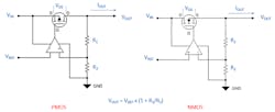
1. The basic PMOS and NMOS linear regulator architectures. (Source: TI Training: LDO Basics—Dropout Voltage video)
Figure 1 shows MOSFET linear-regulator circuits with both PMOS and NMOS power transistors. In both circuits, the voltage across the regulator’s power transistor is:
VDS = VIN - VOUT = IOUT × RDS
where RDS is the FET’s drain-to-source resistance. VDS depends on the FET’s gate-to-source voltage (VGS).


