Say Farewell to Offset Voltage with a Zero-Drift Op Amp

Download this article in PDF format.
As analog engineers, it’s tempting to fantasize about one day coming close to designing the ideal operational amplifier we encountered in college: infinite bandwidth, zero output resistance, and so on. Although it’s a good first-order approximation to simplify analysis, the ideal op amp will remain forever just out of reach, together with ending world hunger, eliminating the National Debt, and the Cubs winning another World Series. Okay, scratch that last one.
Figure 1 shows an ideal op amp model versus its real-world equivalent. As you can see, numerous correction factors are added to bring the model in line with reality. However, the latest real-world designs are getting close to making one of them, offset voltage, a thing of the past in certain applications.
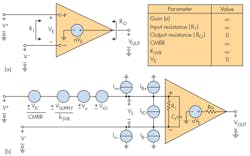
1. The model of a real-world op amp (b) is considerably more complex than its ideal equivalent (a). (Source: Texas Instruments)
Offset Voltage
Offset voltage (VOS) is the differential dc voltage required between the input pins of an op amp to make its output zero. Our ideal op amp has zero volts across its input pins when the output is zero, but in reality, the input terminals are at slightly different dc potentials.
In the model, a voltage source in series with the positive or negative input terminal represents the offset voltage. In real devices, the offset voltage can be negative or positive in polarity and vary from die to die in the same wafer lot.
Input offset voltage is primarily due to the inherent mismatch of the input transistors and components during die fabrication. Stresses placed on the die during packaging also make a minor contribution. These factors cause a mismatch of the bias currents flowing through the input circuit of the op amp, resulting in a voltage differential at the input terminals.
In a typical application, the differential voltage is multiplied by the closed-loop gain of the op amp, which is determined by the external components. Over the years, better matching of components and improved package materials have slowly reduced offset voltages. A trimming procedure during manufacturing is used to reduce the offset voltage, and op amps that exceed the maximum allowable offset voltage after trimming are rejected.
The offset voltage of an op amp drifts over temperature. Offset voltage drift (dVOS/dT) is expressed in terms of the number of microvolts increase per degree of temperature change (µV/°C).
Offset Voltage and Crossover Distortion in Rail-to-Rail Op Amps
Early op-amp designs required dual power supplies (±15 V was typical). The supplies’ input and output voltages could swing to within a volt or so of the rails before running out of headroom. As system voltages declined and battery-powered equipment proliferated, the preferred choice for many precision applications became a low-voltage single-supply op amp that could swing to the supply rail on both input and output, referred to as an RRIO device.
A state-of-the-art device such as Texas Instruments’ new OPAx320-Q1 family of CMOS precision low-voltage RRIO op amps can operate from a single supply of only 1.8 V, or alternatively, a ±0.9-V split supply. The input common-mode range extends 100 mV beyond the supply rails, both positive and negative. The output voltage can typically swing to within 10 mV of the rails.
Achieving rail-to-rail performance requires the designer to make some compromises that affect the offset-voltage performance. As shown in Figure 2, the input circuit of a typical rail-to-rail CMOS op amp has two differential pairs—one PMOS transistor pair (blue) and one NMOS transistor pair (red)—compared to the single pair of a non-RR design.
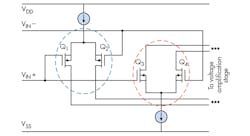
2. The composite input stage of a rail-to-rail op amp contains both PMOS and NMOS differential pairs. (Source: Texas Instruments)
The PMOS transistors can operate with common-mode input voltages from VSS to (VDD-1.8V), and the NMOS transistors can operate with common-mode input voltages from (VDD-1.8V) to VDD. The two input transistor pairs are independent, so their input offset voltages, temperature coefficients, and noise are uncorrelated.
During the transition from the PMOS pair to the NMOS pair, and vice versa, there’s a crossover region at ≈1.8 V below the positive rail where both inputs are conducting (Fig. 3). Within this region, the value of VOS can change—this is a source of distortion known as input crossover distortion.
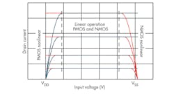
3. Crossover distortion occurs during the transition region, when both sets of transistors are conducting. (Source: Texas Instruments)
For example, the input common-mode voltage (VCM) range of the OPAx316 family of RRIO devices extends 200 mV beyond the supply rails. As Figure 4 illustrates, there’s a pronounced shift in VOS as operation changes from the PMOS to NMOS transistors, and the shift can be in either direction.
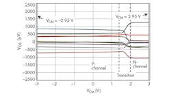
4. Offset voltage and common-mode voltage are compared for nine typical OPA316 RRIO op amps. (Source: Texas Instruments)
This difference shows up in the rail-to-rail op amp data sheet as two or more common-mode rejection ratio (CMRR) specifications.
In Figure 5, the CMRR in dB is equal to 20*log (ΔVCM/VOS). The table shows the CMRR for the OPA316 for two values of supply voltage VS. Note that that for the same test condition, performance is worse when VS = 1.8 V (items 1 and 3) than when VS = 5.5 V (items 2 and 4). The worst CMRR of all, 72 dB typical in item 3, occurs when the OPA316 is in its transition region for almost the entire range of the test.
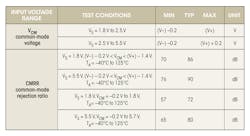
5. RRIO op amps often have multiple CMRR figures to account for the change from PMOS to NMOS operation. (Source: Texas Instruments)
How can we eliminate this crossover distortion? A “zero-crossover” op amp adds an internal charge pump to the input circuitry that raises the top of the differential input to 1.8 V above VDD, the power-supply voltage positive side. Since the PMOS transistors can now operate over the full input range (which hasn’t changed), we can eliminate the NMOS transistors and hence the crossover distortion. Figure 6 shows the improved input stage with the added charge pump.
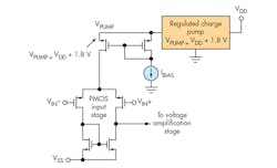
6. Adding a charge pump makes it possible to eliminate the NMOS differential pair and with it, the crossover distortion. (Image Source: Texas Instruments)
Eliminating Offset Voltage: The Zero-Drift Amplifier
Putting another nail in the offset-voltage coffin, zero-drift amplifiers employ a self-correcting technology that provides ultra-low VOS and near-zero drift. This suits them for both general-purpose and precision applications.
Zero-drift amplifiers are good fits for a wide variety of general-purpose and precision applications that benefit from stability in the signal path. The excellent offset and drift performance of these amplifiers make them especially useful early in the signal path, where high gain configurations and interfacing with microvolt signals are common.
It’s possible to optimize system performance with standard continuous-time amplifiers plus a system-level auto-calibration mechanism. However, the method requires complicated hardware and software, and increases development time, cost, and board space.
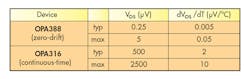
The more efficient solution is to use a zero-drift amplifier such as the OPAx388 family of precision operational amplifiers, available in single, dual, and quad versions. These ultra-low-noise, fast-settling, zero-drift, zero-crossover devices have rail-to-rail input and output operation. The parts feature only 0.25 µV of offset and 0.005 µV/°C of drift over temperature, together with a 1-kHz noise figure of 7.0nV/√Hz and no 1/f noise (140 nV p-p from 0.1 to 10 Hz).
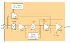
7. Shown is the internal block diagram for the OPA388. (Source: Texas Instruments)
Figure 7 shows the internal architecture of the OPA388. It includes three transconductance amplifiers in the main signal path, plus two chopping networks (CLK1 and CLK2). CLK1 provides initial modulation of the differential input signal up to the chopping frequency; CLK2 both demodulates the input signal and simultaneously modulates the offset and 1/f noise from GM1.
The ripple-reduction block senses the modulated ripple after CLK2 and demodulates it back to dc. It also includes a synchronous notch filter at the switching frequency to attenuate any residual error. The output of the block is then applied to GM1 to null out its offset and 1/f noise.
GM_FF is another transconductance amplifier that provides a feedforward path for high frequencies. The low-noise charge pump supplying the input stage provides zero-crossover performance as mentioned earlier.
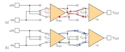
8. In a zero-drift amplifier, the input signal flows through two set of switches. Successive modulation and demodulation null out the error in the input transconductance stage. (Source: Texas Instruments)
Figure 8 shows a simplified switching sequence. Fig. 8a shows the first half cycle: Both sets of switches are configured to flip the input signal twice, but the offset flips once. This keeps the input signal in phase, but reverses the offset error polarity.
Figure 8b shows the second half cycle. Here, both sets of switches are configured to pass the signal and offset error through unaltered. Effectively, the input signal is never out of phase, remaining unchanged from end to end. Since the offset error from the first clock phase and second clock phase are opposite in polarity, the error is averaged to zero when it’s added back into GM1.
9. A zero-drift op amp has considerably better offset performance and drift than a comparable continuous-time device. (Source: Texas Instruments)
Figure 9 compares the offset voltage and drift of the continuous-time OPA316 and the zero-drift OPA388. Notice that the VOS and dVOS/dT are three orders of magnitude smaller on the zero-drift amplifier. The 1/f noise shows a similar improvement (Fig. 10).
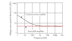
10. The zero-drift topology practically eliminates 1/f noise. (Source: Texas Instruments)
Application Example
Texas Instruments released a reference design that demonstrates the capability of the OPA388 to buffer the analog output of a digital-to-analog converter (DAC) for data acquisition, wireless infrastructure, and test-and-measurement applications. The design shows how the OPA388’s zero-crossover and zero-drift feature operation can minimize the integral nonlinearity (INL) of the system, as well as make use of the full-scale range of the DAC, an ultra-low power 16-bit DAC8830.
Figure 11 shows the reference design block diagram. The REF5050 is a low-noise, low-drift, high-precision voltage reference that’s able to both sink and source current. The device has excellent line and load regulation, very low drift of 3 ppm/°C, and accuracy of 0.05%.
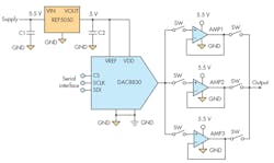
11. This precision DAC reference design uses the OPA388 to buffer a DAC output. (Source: Texas Instruments)
The 16-bit DAC8830 has an LSB voltage of 76 µV when used with a 5-V reference such as the REF5050. The datasheet recommends the use of a low-offset op amp to eliminate the need for offset trimming.
Several op amps can meet the requirements, but the crossover region of a traditional RRIO device will negatively affect the INL, the most important specification for high-precision applications. The zero-crossover capability of the OPA388 allows the INL to remain below 1 LSB across the whole operating range.
Conclusion
Rail-to-rail op amps are widely used in low-voltage precision applications, but traditional input topologies degrade offset-voltage performance in certain operating regions. Zero-crossover devices remedy this shortcoming. Specifically, zero-drift op amps solve the problem of offset drift by adding a switching component to the design.
The advantages of zero-drift op amps over continuous-time devices are particularly pronounced at low frequencies. The op amps are commonly used in applications such as precision strain gauge and weigh scales, current shunt measurement, and thermocouple-, thermopile-, and bridge-sensor interfaces.
Texas Instruments has a broad family of op amps with zero-drift or zero-crossover operation, including the OPA388, which features both capabilities.
About the Author
Paul Pickering
Paul Pickering has over 35 years of engineering and marketing experience, including stints in automotive electronics, precision analog, power semiconductors, flight simulation and robotics. Originally from the North-East of England, he has lived and worked in Europe, the US, and Japan. He has a B.Sc. (Hons) in Physics & Electronics from Royal Holloway College, University of London, and has done graduate work at Tulsa University. In his spare time, he plays and teaches the guitar in the Phoenix, Ariz. area
Comment About the Article
To join the conversation, and become an exclusive member of Electronic Design, create an account today!

Leaders relevant to this article: