Small IS Beautiful: Tiny Packages Help Designers Do More with Less
Download this article in PDF format.
It’ll come as no surprise to any savvy buyer, and certainly not to any design engineer, that each new generation of electronic products packs more performance into a smaller package than the product it replaced (Fig. 1). No matter whether it’s a remote industrial sensor node or the next smart wearable device, space is becoming an increasingly scarce resource.
1. Better not sneeze: Aimed at IoT and personal electronics applications, the TLV9061 consumes only 0.64mm2 and is the world’s smallest op amp. (Source: Texas Instruments)
Sponsored Resources:
- Small size amplifiers for difficult system designs
- Small size data converters break through your toughest design barriers
- Big reductions thanks to tiny packages
Something’s gotta give. In this case, many things. Fitting the increased capability into a smaller volume requires the designer to make improvements in multiple areas. The three biggest keys to succeeding, however, are to reduce the overall power consumption to allow the use of a smaller battery; integrate multiple functions into a single package to cut down on the number of devices; and choose individual components in the smallest available packages.
Manufacturers of both active and passive devices are keenly aware of the push toward smaller sizes. Just look at resistors, for example. Back in the old days before surface-mount technology (SMT), the standard small-signal resistor was a 1/8-W axial through-hole device measuring about 1.8 mm in diameter and 3.0 mm long, plus extra for the leads. The equivalent now is the 0201 surface-mount resistor. Yes, it only handles 50 mW, but it measures 0.3 × 0.6 mm, a reduction in area of 96%.
Integrated circuits are following a similar path. In some cases, manufacturers can reduce the overall size of their products by integrating more functions into a single part. Even single-function devices, though, such as op amps and LDO regulators, are undergoing some serious shrinkage—from leaded dual-inline packages to SOICs to SOT, and below. Traditional packages are much larger than the die they contain, as they must also house the lead frame, the bond wires, etc.
In a chip-scale package, the size of the package approaches the size of the integrated circuit itself. This package requires specialized manufacturing techniques, but brings benefits in addition to smaller size. For instance, the shorter interconnections reduce parasitics, giving improved performance.
Figure 2 shows a selection of packages for devices from 4 to 81 pins, ranging from the plastic dual inline package (PDIP), first introduced in 1964, to current-generation chip-scale offerings. Of course, this isn’t the complete list. It doesn’t include specialized packages, high-power packages, or packages with higher pin counts. The plastic ball-grid-array (PBGA) package can have up to 976 connections!
2. Here are some of the package options available for a single-function device. (Source: TI PDF: Packaging Solutions)
A Real-World Example: Data Acquisition
At the most basic level, a data-acquisition system takes in analog information from the real world, converts it to digital form, and uses the data to produce a desired result. Variations are found everywhere: in the factory, strapped to your wrist, at home, and in the doctor’s office, for example.
A data-acquisition signal chain has several distinct blocks:
- An analog front end (AFE) captures data from one or more sensors and converts it to digital form. This AFE typically includes pure analog components like op amps, and mixed-signal components such as analog-to-digital converters (ADCs).
- A microcontroller receives the data, processes it, and acts on the information.
- A mixed-signal output device such as a digital-to-analog converter (DAC) converts the microcontroller digital output back into analog form, perhaps to power a loudspeaker or actuator
- A power circuit takes input power and provides regulated supplies for all the devices
Although each one of these blocks has benefitted from the move to tiny packages, let’s examine the op-amp and data-converter portion of the signal chain and see how new package options allow designers to dramatically reduce size while simultaneously increasing performance.
Tiny Op Amps Fill Many Roles
As fundamental building blocks in the signal chain, op amps must keep pace with emerging electronic design trends, including the move to successively smaller packages.
How do manufacturers add smaller package options to a part? For existing parts, they simply repackage the device without changing the underlying circuit. The venerable TL071 low-noise JFET op amp, for example, now comes in five different packages. While adding packages, older devices will typically still offer the original package options until the device itself is discontinued—nobody likes a manufacturer who forces them to re-layout their design. But newer devices offer both smaller packages and improved performance.
Portable audio requires tiny devices to produce high-quality sound for smartphones, Blu-Ray players, and headsets. Traditionally, designers have used precision audio op amps in DIP packages for audiophile products. The OPA2134 from the legacy Burr-Brown product line is one such device. It has low distortion, low noise, and has been a professional audio staple over the years.
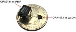
But its PDIP and SOIC packages are an issue for portable applications with severe space constraints. Designers can now choose the OPA1652 (Fig. 3), which features upgraded performance and a smaller package compared to the OPA2134.
3. In addition to a dramatic size reduction, the OPA1652 audio op amp provides superior THD+N performance over the classic OPA2134. (Source: TI Archives: “Achieve big board-size reductions with tiny, precision op amps”)
Performance-wise, the OPS1652 has lower noise (4.5 nV/√Hz at 1 kHz) and lower THD + N (0.00005%) than the OPA2134 (8 nV/√Hz and 0.00008%, respectively).
The OPA1652 is available in several packages, including the WSON no-lead package that features a thin profile for handheld applications. The OPA1652’s version (DRG package code) has an exposed thermal pad and measures 3.0 × 3.0 mm—much smaller than the OPA214’s standard PDIP package (6.35 × 9.81 mm).
For general-purpose use, the OPA171 is worth considering. It’s is one of the first micropower 36-V op amps offered in both a single SOT553 (1.6 × 1.6 mm) package and a dual, very-thin shrink small outline package (VSSOP) (2.0 × 3.1 mm).
In addition to changing to tiny packages, new op amps are adding specialized features for new applications. Many battery-powered products spend much of their time in sleep mode and wake up periodically to perform scheduled operations, process an incoming message, or respond to an interrupt. A fitness band, for example, only wakes up to measure biometric data; when the user presses a button; or when pinged by a paired smartphone.
Conserving battery life is a top priority in these applications. In sleep mode, it’s important to shut off as many devices as possible. While awake, the device must only power the blocks that are needed for the operation being performed.
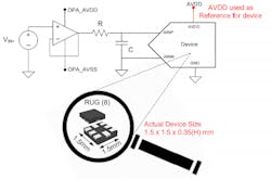
These requirements have led to low-power op amps with a shutdown feature. The OPA2316S, for example, is a low-power CMOS op amp with a bandwidth of 10 MHz. The part operates down to 1.8 V and offers rail-to-rail input and output (RRIO) operation, making it suitable for low-voltage battery-powered devices. In shutdown mode, the OPA2316A consumes 0.01 µA typical. For the smallest size, it comes in a quad flat-pack no-lead (X2QFN) package measuring 1.5 × 2 × 0.4 mm.
Data Converters: Linking the Analog and Digital Worlds
The ADC and the DAC are two important blocks in the signal chain. Analog-to-digital conversion occurs on the input side; tiny packages are appearing in this category as well.
Numerous data converters are available in tiny packages. Here are a couple of examples.
The ADS7040 is an ultra-low-power, 8-bit ADC that targets low-power data-acquisition, portable medical, and wearable applications, among others (Fig. 4). This device also comes in the X2QFN package. Although it uses the successive-approximation register (SAR) architecture to achieve 1 Msample/s, the ADS7040 consumes only 171 µW when powered by a 1.8-V battery cell.
4. The ADS7040 shrinks a 1-Msample/s SAR ADC down to 2.25 mm2. (Source: TI PDF: ADS7040)
On the output side of the house, the DACx0504 is a pin-compatible family of low-power, four-channel DACs with 16- and 14-bit resolution and buffered voltage outputs. The DACx0504 includes a 2.5-V, 5- ppm/°C internal reference, eliminating the need for an external precision reference in most applications.
The device operates from a single 2.7- to 5.5-V supply, is monotonic, and provides ±1 LSB integral nonlinearity (INL) performance. The DACx0504 communicates via a 4-wire SPI-compatible serial interface at up to 50-MHz clock rate. Best of all, the DACx0504 is available in a 16-pin WQFN package (package code RTE) that measures 3.0 × 3.0 mm.
Layout Guidelines for Small Packages
Using tiny packages allows you to shrink the size of the design, but the small package dimensions leave very little room for error. It’s important to follow manufacturer’s recommendations when laying out the printed-circuit board (PCB) and later during manufacturing. Texas Instruments offers application notes that provide guidance for many tiny packages.
Three primary factors can make the difference with regard to package size and pitch: PCB manufacturing, solder application, and component placement.
Here are some general rules, using the Extra Small Outline No-Lead (X2SON) package as an example. This package comes in 5-pin (code DPW) and 6-pin (DTB) versions that measure 0.8 × 0.8 mm and 0.8 × 1.0 mm, respectively. These packages are used by both logic and analog devices including the TLV9061 shown in Fig. 1, a 10-MHz CMOS op amp that finds homes in many consumer and industrial applications.
PCB Manufacturing
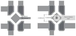
The PCB footprint for the X2SON packages requires a spacing of 0.208 mm (8.2 mils), which is well within the limits of most established PCB manufacturers. The primary manufacturing concern comes from the method used to connect to the center pin(s).
There are two layout options for the center pin: place a trace on the same layer as the other pins; or use a via to connect to a trace on another layer. Figure 5 shows recommended clearances in each case. Consult the guidelines in the application note for more information.
5. Shown are recommended layout clearances for the X2SON center pin: trace on same layer (left) and trace on separate layer (right) (Source: TI PDF: “Designing and Manufacturing with TI’s X2SON Packages”)
Solder-Paste Application
Solder-paste application is an area of concern when the pads are very small. For instance, the correct amount of solder needs to be placed on the pads. There are several variables, including stencil thickness, solder type, and aperture size and shape. However, the X2SON packages maintain a 0.4 mm (15.7 mils) pitch, which allows for more error in the assembly process while maintaining a high yield. When following recommended guidelines, industry-standard Type III solder paste can also be used.
Component Placement
Using a one-third pad placement error as a guideline, the X2SON-5 package requires a minimum placement accuracy of ±83 µm (3.28 mils) to seat the part properly; the X2SON-6 requires an accuracy of ±72 µm (2.94 mils). The one-third pad error tolerance enables all pins to make good contact with the solder paste and be in reasonable alignment with their pads. During the solder process, the surface tension of the melted solder will align the part. Pick-and-place machines can typically place a component with an accuracy of ±30 µm, well within the requirements for the X2SON.
Resources and Information
Application guidelines are available for many of the newer tiny packages. AN-1112, for example, covers the die-size ball-grid-array (DSBGA) wafer-scale package. The complete list can be found here, including information on older through-hole and power packages.
For analog and logic devices, you can browse through the Analog and Logic Packaging guide. It lists all of the available packages by pin count, with photographs of each one. Find out more about TI’s broad packaging portfolio at this link.
Sponsored Resources:
About the Author
Paul Pickering
Paul Pickering has over 35 years of engineering and marketing experience, including stints in automotive electronics, precision analog, power semiconductors, flight simulation and robotics. Originally from the North-East of England, he has lived and worked in Europe, the US, and Japan. He has a B.Sc. (Hons) in Physics & Electronics from Royal Holloway College, University of London, and has done graduate work at Tulsa University. In his spare time, he plays and teaches the guitar in the Phoenix, Ariz. area


