Download this article in .PDF format
Phase-locked-loop (PLL) frequency synthesizers are signal sources often employed in many types of electronic equipment. They show up as clock sources in high-frequency instruments and as local oscillators in a variety of radios and wireless gear. Instrument examples include oscilloscopes, signal waveform generators, vector signal analyzers, and communications test sets. Among the wireless applications are land mobile radios, cellular base stations, microwave backhaul units, and most software-defined radios.
These single-chip signal sources are at the core of your design, so performance is critical. Here’s a brief overview of these ICs and a related discussion of the importance of phase noise.
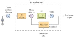
Figure 1 shows the basic building block of a PLL frequency synthesizer. The output, which may be a rectangular wave or sine wave, is derived from the voltage-controlled oscillator (VCO). All of the remaining circuits are used to determine the output frequency. Note that the circuit is a closed-loop feedback system.PLL Synthesizer Operation
The initial input comes from a crystal-oscillator reference source that sets the precision and accuracy of the PLL. Its frequency is some sub-multiple of the final VCO output. The reference oscillator feeds a frequency divider that may be fixed or variable. It divides the oscillator output by factor R so that it will match the feedback from the VCO and the other frequency divider.
The R divider drives a phase detector; a second input to the phase detector comes from the N divider. Both detector inputs are at the same frequency. The detector is sensitive to the phase shift between the two inputs. The output is a pulse sequence proportional to the phase difference between the two inputs. The pulse train is smoothed into a dc voltage by the low-pass filter (LPF)—this is the control voltage that varies the VCO output frequency.
The VCO output is sent to the N frequency divider that determines the PLL synthesizer’s final output frequency. The division factor N is adjustable in increments and set by an external input. This allows the output frequency to be set on the fly in a desired step increase or decrease.
One example of how to determine the output frequency: Assume a desired final output of 200 MHz. Also say that the reference crystal-oscillator output is 10 MHz and divider R is set to 10. The input to the phase detector then is 1 MHz.
To stabilize the loop, or as we say “locked,” the phase-detector input frequencies must be equal. This means that the output of divider N must also be 1 MHz. Setting N to 200 will meet this condition.
Now if N is changed to 201, the phase-detector input frequencies do not match. As a result, the phase detector develops a dc output that drives the VCO output frequency higher or lower until the loop returns to lock. With N at 201, the VCO output must be increased to 201 MHz. Note that a one-increment change in N results in a 1-MHz increment change in output.
Keep in mind that the output of divider R sets the change increment of the PLL synthesizer. This type of synthesizer is called an integer-N PLL synthesizer. Other divider arrangements like fractional-N are possible to provide greater flexibility in setting the output frequency.
Many different types of PLL ICs are available, with most of the newer designs incorporating the VCO. In older designs, the VCO was a separate chip. Another off-chip necessity is the LPF loop filter, which consists of resistors and capacitors. This filter is designed to optimize the loop response. An external crystal reference oscillator is also needed.
The key specifications are output-frequency range and phase noise. The lowest output is usually from 10 to 50 MHz rwith an upper frequency in the 4- to 12-GHz range. Phase-noise figures range from about –115 to –231 dBc/Hz with a 100-kHz offset.
The Importance of Phase Noise
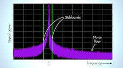
When you look at the VCO output of a PLL on a spectrum analyzer, you should see a single thin vertical line representing the sine-wave output at some frequency. Actually, this should be the case for the output of any sine-wave signal source, such as a crystal oscillator. It represents the ideal scenario under perfect conditions.
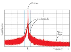
In reality, though, what you actually observe is something like that shown in Figure 2. The sine wave called the carrier is shown, of course, but around it are other signal frequencies below and above the sine wave or carrier frequency. These surrounding signals are sidebands caused by phase noise. The noise floor appears on either side of the signal.
Phase noise is the minor variation of the carrier signal’s phase and amplitude. Noise comes from external sources such as semiconductor devices, power supplies, or thermal noise from other components. Essentially, this noise phase- and amplitude-modulates the carrier. This effect manifests itself in frequency modulation that produces the sidebands.
Phase noise is detrimental to the performance of any PLL synthesizer and any transmitter or receiver that incorporates the synthesizer. Phase noise produces a fuzzy carrier signal that when further modulated can produce data errors. The effect is very serious at the higher carrier frequencies and fast data rates. In a receiver, the phase noise can mask low-level signals, resulting in lower sensitivity and signal-recovery errors.
A particularly onerous problem is generated by the PLL circuit itself. The PLL is a frequency multiplier, since it multiplies the reference input to the phase detector by a factor determined by the N divider. As a result, any phase noise from the crystal oscillator is multiplied by the same amount. Therefore, it’s critical to start with an input oscillator that has the lowest-possible phase noise.
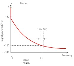
Phase noise is usually plotted as shown in Figure 3. This graph shows the average noise power of the upper sidebands (lower sidebands are essentially equal). The noise power is averaged over a 1-Hz bandwidth offset from the carrier. The offset is usually some decade value from 1 kHz to 10 MHz (a common offset is 100 kHz). The actual value is a measure of the size of the noise compared to the carrier power (the measurement unit is dBc/Hz).
In Fig. 3, the phase noise is –120 dBc/Hz at a 100-kHz offset. The larger the negative value, the lower the phase noise.
Total phase noise for a PLL synthesizer is the sum of the flicker noise, flat noise, and PLL open-loop noise. Flicker noise, also called pink or 1/f noise, is a random noise generated inside semiconductor devices by carrier movements. Flat noise or white noise is generated by thermal agitation in components. Open-loop noise is a value that PLL manufacturers put in their datasheets. To get the correct total phase noise, the noise values must all be normalized. This article shows how to do the calculations.
Selecting a PLL Synthesizer IC
Many new fully integrated PLL synthesizers are now available. With wide frequency ranges and impressively low phase noise, these ICs make new designs faster and simpler. What was once a complex and tedious design process is now reduced to selecting amongst multiple available devices. In most cases, evaluation boards are also available for initial testing. Some product suggestions can be found in this article.
Looking for parts? Go to SourceESB.


