
Download this article in PDF format.
In 2007, a power-conversion startup company was promoting a wall-wart schematic that had an external FET driving an external high-voltage transistor (Fig. 1). I note the startup company has been absorbed by the great folks at Power Integrations, and I see no mention of this part or schematic on its website. Indeed, Power Integrations confirmed it has obsoleted the part, and would recommend its LinkSwitch-4 device, which drives a HV transistor directly via the base.
When I first saw this external FET circuit in 2007, I did not understand the reason, thinking that it would be easier to put the FET inside the package or have the internal FET drive a bigger external FET. I was also confused as to why the driver FET was connected to the HV transistor in a common-base configuration. I tried asking a PR person from the startup company, but he really did not have any definitive answer. I then wrote a bunch of pals asking what was going on.
To my question of “why don't they just drive the base directly with the chip?” Bob Pease wrote, “I think I can answer that. The base of the low-beta NPN would be harder to drive than driving the FET through the emitter. With the base driven, you would need to drive more base current and more Miller current. The FET helps avoid that.”
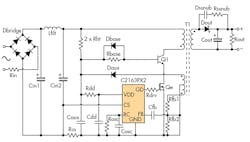
1. This offline low-power flyback converter uses a FET to drive a transistor in common-base mode.
The Miller effect is caused by the unavoidable capacitance between a collector and the base, or the drain and the gate (Fig. 2). As the transistor turns on, the collector voltage will start to drop. The CB (collector-base) capacitance will try to drive the base lower, impeding its turn-on. The faster the signal, the more the base is driven low. This can be worse in large FETs, since the DG (drain-gate) capacitance tends to be larger than the CB capacitance of a similar NPN transistor.
Pease continued,
“Hello, Gentlemen, and Paul, too. I think this PR person is just playing dumb, and mouthing what he was told to say, ‘The output transistor is just a cheap bipolar’ for PR effect, and to distract the customer with half-truths. He probably finds it easy to play dumb, because he is dumb. The real engineers avoided telling him because they want him to stay dumb. You are correct to question him—and to ask us. I think this is just a matter of partitioning. All the rest of the circuit is low-voltage CMOS, such as 5 or 12 volts. (It's hard to be sure as there are no R values published.) By using ONE cheap high-voltage NPN, 2N3440 or similar, they don't need a high-voltage FET process on their chip. I think this is a reasonable cost-effective solution. It is a reasonable example of ‘dis-integration.’ When is it new for PR guys to take a forced decision, and present it as a brilliant advantage? Let me go back and see if that ain't my position. Yeah. That's my analysis. Beast [sic] regards. / rap”
This makes sense. To have an IC process that has 250-V breakdown voltages will penalize every device inside the chip and add size and cost to the die. I saw this with DSL amplifiers. Telecom companies did not integrate the driver amps inside the logic chips. The amplifiers were transformer-coupled to a twisted-pair POTS line that might be kilometers long. So the amplifiers needed large electrostatic-discharge (ESD) diodes to clamp the spikes and noise coming in from those wires. It is better to use a wide-line analog process for that, and to penalize the amplifier die, rather than put large ESD diodes on a fine-line CMOS logic chip where the die real estate is much more expensive.
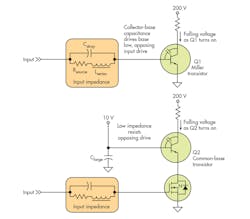
2. The circuit of Q1 is subject to the Miller effect. As the collector voltage falls during turn-on, the internal capacitance inside the transistor applies that dropping voltage to the base, which tends to turn it back off. Q2 is driven by a FET using the transistor in common-base mode. The lower impedance at the base better resists the Miller effect.
Pease wrote me later and added. “Here's another tidbit. NPN's and bipolars saturate, and if driven directly, they Miller a lot. FETs are easy to drive to their dc levels, but their gate-drain capacitance can be very big. Lots of Miller effect.”
Meanwhile Bob Dobkin, CTO of Linear Technology, wrote me, “The main reason to have a FET drive a bipolar is cost. Bipolars are cheaper than HV FETs. The FET is used by the IC because it is easier to drive. But I bet the cost of both devices, assembly and stocking, are more than one HV FET. Also, HV bipolars are slow compared to FETs. So the transformer and capacitors are larger.”
That is what I could not get the PR guy to explain. I said he had to give me Digi-Key pricing to show that one HV FET was more expensive than one HV transistor plus one LV FET. I now get why they drove the transistor common-base. Yanking on the emitter reduces the Miller effect. It takes less gate drive to charge the gate of a LV FET with a Miller swing of maybe 10 V, rather than directly drive a HV transistor where the Miller swing will be hundreds of volts.
That is a feature of these parts—good efficiency—so maybe they can save some coulombs of gate drive, too. But still, that does not mean they don't have a cost penalty for the FET + transistor. The PR guy said Digi-Key pricing was not representative, so I asked him to give me Arrow or Farnell or any other high-volume pricing.
Soon Jon Dutra, then a Texas Instruments application engineer and now at Apple, added, “There is still a Miller effect even if the bipolar is driven common-base, unless the base impedance is zero, which it is not. But the bottom FET does not see the high dV/dt so it is a faster way to drive, no Miller effect, at the expense of part count and V*I losses when on. To Dobby’s [Dobkin’s] point, some clamp diodes are likely in order, as when Williams did the cascode in Figure 6 of AN25 (Fig. 3). The corner cases, and line and load transients, will tell the tale of reliability. The data sheet of this device tells you more about their algorithm. It looks like it could work. I am surprised they ac-coupled the FB [feedback] pin. They don't give a part number for the cascode NPN in any of their data sheets. At low power, an NPN cascode on top of a FET or NPN, should be fine.”
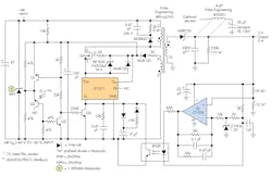
3. Jim Williams used a cascode common-drain arrangement in this fully-isolated −48- to +5-V regulator. The 100-μF capacitor creates the low-impedance gate bias voltage, but Williams was careful to add a clamping diode and Zener to the gate. (Courtesy of Linear Technology)
Dobkin added, “I have seen another problem with HV transistors. They are slow. If you turn off the emitter, all the current in the transistor has to go somewhere. Some comes out the base, some comes out the emitter. If you turn off fast enough, the emitter will fly high and blow out the FET below it. You cannot run this circuit fast. If you turn off the FET fast, the current in the bipolar continues to flow. The emitter goes high until it breaks down the EB [emitter-base] junction or the FET. In either case you are going to eventually let the smoke out of the package.”
Pease agreed, “Dobkin is quite right, the emitter could go high. That's why they put the clamp diode on the NPN's base, to help hold down the base—and thus the emitter. When a saturated transistor has its collector go to well over 100 volts, the collector-base capacitance will try to take the base and emitter with it. But the clamp on the base may help a lot—it can help pull the saturated base-emitter junction off. / rap”
Pease added,” The impedance at the base of the NPN is easy to make lower than the impedance of the driver for the FET gate. So the FET driver can be small, and has to drive almost no Miller capacitance. The cascode lets you avoid the Millering problem. The base (or gate) tied to the +12-volt bias can pump a lot of current into the +12-V bias bus, but that's a low impedance, and cheap. The drive to the gate of the FET is much more delicate than the drive to the base of the cascode. / rap”
So it seems this schematic was a good architecture to limit the Miller effect, but hampered by an IC process that could not integrate a high-current FET. Interestingly, when I look at low-cost ICs for wall-warts, I see most of them drive a HV transistor base directly, like the LinkSwitch-4. Therefore, most companies must have a process that has such a low impedance output where the Miller effect is not a problem. Cost is king in these applications, and it makes sense to reduce the parts count as much as possible.
Pease ended with a critique of marketing techniques that don’t give precise information, “P.S. The schematic you showed us is a simplified schematic. I bet there are R-C dampers somewhere in the real circuit. To heck with a PR guy who tries to argue that ‘This schematic shows how smart we are...’ People who wave around simplified schematics aren't worth much. / rap”
About the Author

Paul Rako
Creative Director
Paul Rako is a creative director for Rako Studios. After attending GMI (now Kettering University) and the University of Michigan, he worked as an auto engineer in Detroit. He moved to Silicon Valley to start an engineering consulting company. After his share of startups and contract work, he became an apps engineer at National Semiconductor and a marketing maven at Analog Devices and Atmel. He also had a five-year stint at EDN magazine on the analog beat. His interests include politics, philosophy, motorcycles, and making music and videos. He has six Harley Sportsters, a studio full of musical instruments, a complete laboratory, and a video set at Tranquility Base, his home office in Sun City Center Florida.
Comment About the Article
To join the conversation, and become an exclusive member of Electronic Design, create an account today!

Leaders relevant to this article: