What’s The Difference Between Continuous-Time And Discrete-Time Delta-Sigma ADCs?
This file type includes high resolution graphics and schematics when applicable.
Discrete-time analog-to-digital converters (ADCs) implemented using switched-capacitor circuits have been the designer’s choice for the last few decades. These ADCs offer high precision and accuracy, making them a good selection for applications like weigh scales, temperature measurement, and biopotential measurement.
Yet recently, continuous-time delta-sigma ADCs have gained popularity in technical journals and the industry. They have been used in communications chips where inherent anti-aliasing provided by the continuous-time architecture is very useful.
Discrete-Time Delta-Sigma ADCs
Delta-sigma ADCs are oversampling ADCs that sample the signal at much higher rates than a Nyquist rate. For a signal with maximum bandwidth, fB, the Nyquist theorem states that input must be sampled at a rate > 2fB. The ratio of sampling frequency (FS) to twice the signal bandwidth (2fB) is called the oversampling ratio (OSR).
In a discrete-time delta-sigma ADC, sampling of the input signal x(t) occurs prior to the loop filter (Fig. 1). The loop filter H(z) is discrete time, implemented using switched-capacitor integrators. The quantizer generally is low resolution, somewhere from 1 to 5 bits. The loop filter shapes the quantization noise out of the baseband to higher frequencies.
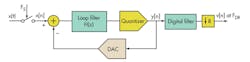
The feedback digital-to-analog converter (DAC) is also discrete-time implemented with switched-capacitor techniques. The loop filter does not shape errors in the feedback DAC, requiring the DAC to be as good as the overall ADC. The output of the quantizer is low-pass filtered by a decimation filter, which outputs the data at the rate of FDR.
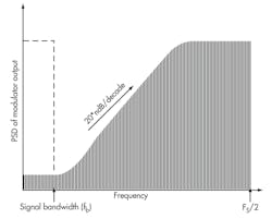
Figure 2 illustrates the power spectral density (PSD) of the output y[n] of a typical delta-sigma ADC. The noise-shaping slope depends on the order of loop filter H(z) and is 20*ndB/decade where n is the order of the loop filter. The delta-sigma ADC achieves high resolution in band fb by a combination of noise shaping and oversampling. Higher resolution can be obtained by increasing the order of the loop filter or by increasing the oversampling ratio.1
Continuous-Time Delta-Sigma ADC
In a continuous-time delta-sigma ADC, the principle of noise shaping and oversampling remains the same as its discrete-time counterpart (Fig. 3). The key difference is where the sampling operation takes place. In the continuous-time design, input sampling takes place just before the quantizer. The loop filter is now continuous-time using continuous-time integrators, often RC or gm/C integrators.
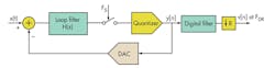
This is in contrast to the switched-capacitor integrators used for a discrete-time ADC. The feedback DAC can be implemented either in discrete time using switched-capacitor circuits or in continuous time using a current-steering DAC.
The DAC architecture choice is critical and affects the performance of a continuous-time ADC. There are key differences between a discrete-time DAC using switched-capacitor circuits and a continuous-time, current-steering DAC.
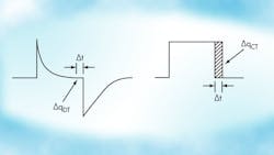
The current-steering DAC is more sensitive to clock jitter than a switched-capacitor DAC. With a switched-capacitor DAC, the bulk of the charge is transferred to the integrator at the onset of integration phase, and a very small charge is transferred towards the end on the integration phase (Fig. 4). An uncertainty in the integration time period due to clock jitter leads to a very small error in total charge integrated in the switched-capacitor DAC.
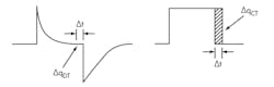
For a continuous-time design with current source feedback, a constant charge is transferred to the integration capacitor during the entire integration phase. This leads to significant noise, if the feedback clock has jitter associated with it. Clock jitter directly modulates the feedback signal and can cause noise folding over the desired signal bandwidth.
Also, bandwidth requirements on the first integrator operational amplifier (op amp) are relaxed with the use of current-steering DACs. That’s because there are no step inputs to the op amp with this DAC architecture. With a switched-capacitor DAC, the op amp sees a step input that must settle within half a clock cycle, leading to high-bandwidth requirements, which then leads to higher power consumption. Additionally, current-steering DACs are more prone to intersymbol interference because of asymmetric rise and fall times on the feedback clock versus switched-capacitor DACs.2
Continuous-time ADCs commonly employ continuous-time DACs in their feedback to reduce power consumption and enable high-speed operation. However, using a switched-capacitor DAC in a continuous-time ADC architecture can relax the jitter requirements on the clock significantly.
Advantages Of Continuous-Time Delta-Sigma ADCs
The input signal x(t) in Figure 1 is sampled at frequency FS. To prevent the input signal from aliasing back into the signal bandwidth of interest, the input signal must be band-limited to FS/2 frequency. This requires an anti-aliasing filter before the discrete-time ADC to suppress the signal content near FS and multiples of FS.
Looking at Figure 3, we observe that the input signal first passes through the loop filter before being sampled. This loop filter now acts as an anti-aliasing filter, relaxing the requirement on any external anti-aliasing filter. Furthermore, since the aliased signals are injected at the input of the quantizer, the loop filter attenuates them in the same way as quantization noise. The order of anti-aliasing achieved depends on the loop filter architecture.
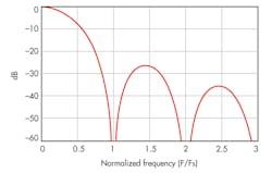
A second-order sinc filter is an example signal transfer function (STF) of a continuous-time ADC with second-order loop filter with all poles (Fig. 5). For an nth order loop-filter with all pole transfer functions, nth order anti-aliasing is obtained. For loop filters with feed-forward, the path order of anti-alias filtering obtained is reduced. However, at minimum, first-order anti-alias filtering is always obtained.3 Thus, a continuous-time ADC can be considered a combination of an anti-aliasing filter and an ADC.
Also, the discrete-time delta-sigma ADC places stringent settling time requirements on its input driver. The sampling clock FS typically is divided into two non-overlapping phases: φ1 and φ2 (Fig. 6). During the φ1 phase, the sampling capacitor, CS, gets connected to the input driver.
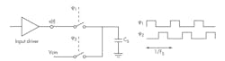
The act of switching the sampling capacitor causes a step at driver output, causing the driver output to deviate from its ideal value. The driver must have sufficient bandwidth to settle back to desired accuracy within the φ1 phase. This leads to increased power consumption in the input driver.
Since the continuous-time design moves the sampling away from the input, the continuous-time ADC doesn’t present a switching load to the input driver. This relaxes the bandwidth specifications on the driver.
In addition, continuous-time delta-sigma ADCs typically consume less power than discrete-time ADCs for comparable noise performance. In a discrete-time ADC, the sampling operation with its associated noise foldover places a fundamental limit on the maximum achievable dynamic range for a given value of the sampling capacitor and oversampling ratio.
The sampling circuit in Figure 6 samples a noise power equal to kT/CS in the sampling phase. Similarly, in the φ2 phase, the integrator as well as the switch noise folds over to provide another αkT/C term.
The exact value of α depends on the integrator implementation. In the continuous-time ADC, the noise of the op amp in the integrator does not fold over, which potentially can lower the op amp’s power consumption.
Another factor that helps reduce power is that the integrators in the continuous-time design are not switched. As a result, they do not have stringent settling and slew requirements, leading to lower power consumptions.4
Note that op-amp bandwidth requirements on the first integrator are relaxed only if the feedback DAC is implemented as continuous time. If the feedback DAC is implemented as a switched capacitor, the op-amp settling requirements are the same as they are for a discrete-time ADC design.
In a discrete-time design, the loop filter consists of discrete-time integrators that are clocked at the sampling rate, FS. The op amp’s settling time used in these integrators sets an upper limit on the maximum clock frequency for a given technology node.
In the continuous-time design using a current-steering DAC, only the quantizer is clocked. Since quantizers typically consist of only open-loop comparators, they can be clocked at a higher clock frequency than the switch capacitor integrators.
In a discrete-time design, the jitter on the input sampling clock limits the maximum possible signal-to-noise ratio (SNR) achieved by the ADC. For a Nyquist rate ADC, assuming the jitter noise is white with rms value ε, SNR is limited to:5
SNR = –20log10(2π*ε*fIN)
For the oversampled ADC, the SNR is limited to:
SNR = –20log10(2π*ε*fIN) + 10log10(OSR)
For a continuous-time ADC, sampling takes place after the loop filter, which relaxes the jitter requirement on the sampling clock. The loop filter shapes the error introduced by the sampling jitter. The continuous-time ADC with switched-capacitor feedback DAC has a relaxed jitter requirement on both the sampling and feedback DAC clock.
Disadvantages Of Continuous-Time Delta-Sigma ADCs
Continuous-time delta-sigma ADCs can only operate at a fixed clock frequency, FS. The pole locations of the integrators do not scale with frequency as in discrete-time design. This limits the use of continuous-time delta-sigma ADCs as a catalog part where customers expect to use a wide range of clock frequencies in the system. As a result, continuous-time ADCs are mostly successful as a part of large system-on-chip (SoC) designs where the clock is well defined and not readily changed.
Additionally, the STF is not flat for a continuous-time ADC (Fig. 5, again). For the discrete-time ADC, the STF for the analog portion is generally flat and dominated by the magnitude response of the decimation filter. Continuous-time delta-sigma ADCs also exhibit out-of-band peaking in the STF for feed-forward architectures.3
This is especially detrimental because it limits the useful input signal range for the ADC. In communications applications, with large out-of-band interferers, it can cause the ADC to become unstable. For these applications, it may be necessary to filter the interferers or sacrifice some of the ADC’s dynamic range, if the feed-forward architecture is used.
Usually, continuous-time ADCs also have a limited common-mode rejection ratio (CMRR) because of mismatch in the input resistors or input transconductance. The common-mode level at the first integrator inputs directly depends on the external input common-mode level as well. This may limit the common-mode input range for the continuous-time ADC.
In contrast, the dc common-mode level for the integrator in discrete-time ADCs can be easily decoupled from the input common-mode level by the sampling capacitor. Also, proper sampling techniques in discrete-time ADCs can provide very large CMRR.
The feedback DAC path and clock jitter depend on the DAC architecture used in the continuous-time ADC, as discussed earlier. The most common implementations of continuous-time ADCs use continuous-time current-steering DACs to reduce power consumption on the integrators. These DACs are more susceptible to clock jitter than a switched-capacitor DAC. The discrete-time ADC always uses switched-capacitor DACs and does not have a stringent jitter requirement on the feedback DAC clock.
Summary
The continuous-time delta-sigma ADC design extends the bandwidth achievable with delta-sigma technology. The industry’s fastest discrete-time delta-sigma ADC, the ADS1610, has a signal bandwidth of 5 MHz. The continuous-time technology has enabled products like the ADC12EU050, which can provide alias-free sampling bandwidth up to 22.5 MHz. The continuous-time architecture has the potential to achieve even higher bandwidth by taking advantage of advanced process nodes.
The continuous-time ADC continues to gain popularity against pipelined ADCs in communication applications because of its inherent anti-aliasing feature. Continuous-time designs have not been used extensively yet for precision dc-type applications where discrete-time delta-sigma designs still dominate. The inability to change the ADC sampling clock as required by the system is the biggest drawback limiting the use of continuous-time ADCs in dc-type applications.
Reference
1. Richard Schreier and Gabor C. Temes, Understanding Delta-Sigma Data Converters, John Wiley and Sons, 2005
2. James A. Cherry and W. Martin Snelgrove, Continuous-time delta-sigma modulators for High-speed A/D conversion Theory, Practice and Fundamental Performance Limits, Springer, 1999
3. Lucien Breems and Johan Huijsing, Continuous Time Sigma Delta Modulation for A/d Conversion in Radio Receivers, Springer, 2001
4. Shouli Yan, Baseband Continuous-Time Sigma-Delta Analog-to-Digital Conversion for ADSL Applications, PhD thesis, Texas A&M University, 2002
5. Behzad Razavi, Principles of Data Conversion System Design, Wiley IEEE Press, 1994
6. Download these data sheets: ADS1610, ADC12EU050
Amit Kumar Gupta is an analog system architect at Texas Instruments, where he defines next-generation products for the Delta-Sigma ADC product line. He received his MSEE from Texas A&M University, College Station, Texas, and PhD from University of Texas, Austin. He has been granted four patents and is a member of TI’s Group Technical Staff and a senior member with IEEE. He can be reached at [email protected].
About the Author
Amit Gupta
Amit Kumar Gupta is an analog system architect at Texas Instruments, where he defines next-generation products for the Delta-Sigma ADC product line. He received his MSEE from Texas A&M University, College Station, Texas, and PhD from University of Texas, Austin. He has been granted four patents and is a member of TI’s Group Technical Staff and a senior member with IEEE. He can be reached at [email protected].
Comment About the Article
To join the conversation, and become an exclusive member of Electronic Design, create an account today!

Leaders relevant to this article: