Automotive systems like advanced driver-assistance systems (ADAS) make heavy use of many types of sensors including cameras. Vision systems are also key elements in many other embedded applications from robotics to surveillance. Higher-resolution cameras generate a better-quality image, but these also require more processing.
However, adding an FPGA to the mix allows processing up front that can reduce bandwidth requirements and add functionality at the source. This can be a boon to many applications, from drones to augmented- and virtual-reality headsets.
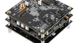
1. Lattice Semiconductor’s CrossLink Video Interface Platform (VIP) Bridge Board includes a CrossLink FPGA and a pair of IMX214 camera sensors.
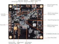
On that front, Lattice Semiconductor’s CrossLink Video Interface Platform (VIP) Bridge Board (Fig. 1), which is part of the company's Embedded Vision Development Kit, includes a CrossLink FPGA and a pair of IMX214 camera sensors. Two cameras can be used to implement stereo vision systems as well as other single- and dual-camera applications. It has four user-programmable LEDs and on-board SPI flash for the FPGA.
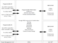
The FPGA can handle video chores such as multiplexing and demultiplexing, merging video streams, arbitration, splitting, and data conversion. It’s also capable of delivering custom data stream protocols.
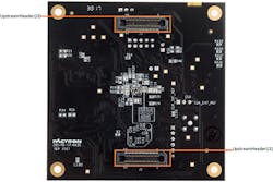
2. The back of the VIP board has a pair of connectors that enables a carrier board to access the processed video.
The VIP board provides a front-end FPGA processing system that’s often connected to a host like the ECP5 VIP processing board. The two upstream connectors on the back (Fig. 2) enable access to the CrossLink FPGA I/O.
The CrossLink FPGA (Fig. 3) is based on Lattice’s 40-nm, low-power FPGA technology. It includes 5,936 lookup tables (LUTs), a pair of MIPI D-PHY interfaces, a hard core I2C/SPI interface, as well as programmable and general-purpose I/O ports. The MIPI interfaces operate at speeds up to 6 Gb/s. They support four data lanes and have one clock lane. The system can handle video streams up to 4K UHD.
3. The CrossLink FPGA includes 5,936 LUTs, a pair of MIPI D-PHY interfaces, a hard core I2C/SPI interface, plus programmable and general-purpose I/O ports.
Lattice offers a number of IP modules for the FPGA, all of which are supported by the Lattice Diamond development tools. The Diamond license is free for non-SERDES devices. The FPGA can be programmed using the on-board header or via one of the upstream connectors. Each camera has its own I2C programming interface connected to the upstream connectors. On-board regulators support power inputs of 5, 3.3, or 2.5 V.
This board is not available separately but is normally part of Lattice's video kits. I will be checking out some of Lattice’s video kits in the near future, so stay tuned.


