This file type includes high-resolution graphics and schematics when applicable.
High-speed serial interfaces are the primary I/O architecture of most of today’s communications products. Virtually all electronic devices in use now incorporate fast serial data transfers. Examples include ASIC and FPGA connections on a printed-circuit board (PCB), board-to-board connections, or short cables. Multiple interface standards exist to carry such data.
PCIe is used in computers, SATA and SAS generally target storage products, and Ethernet is employed in networking. Other serial standards are used in telecom, medical, and consumer products. And gigabit data speeds are the norm. With serial rates up to 28 Gb/s and more, the design challenge is maintaining signal integrity over any distance. Careful design of the signal path and the inclusion of equalization have proven to produce the desired result.
Goals of Signal Integrity
The main design objectives of any serial link are a low bit error rate (BER), minimal jitter, and no inter-symbol interference (ISI). Typical BERs are in the 10-10 to 10-18 range. Jitter is the rapid time shift in the leading and trailing edges of a pulse. It’s similar to a low-deviation frequency modulation caused by clock instability, PLL variations, and noise. Jitter is measured by averaging bit interval variations, usually in picoseconds. ISI is the condition where adjacent bits in the serial pulse train lap over and interfere with one another due to signal distortion, causing bit-interpretation errors.
These design objectives are achieved with a well-designed signal path. That includes the physical path as well as any corrective circuits added to the path. Corrective circuits include equalizers, repeaters, and retimers.
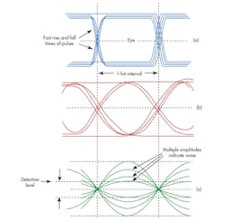
A common measurement of good signal integrity is the eye diagram, which is an oscilloscope display of repeating and overlapping bit time periods (unit intervals or UIs) (Fig. 1). The rise and fall times define the pattern.
With fast rise and fall times, the “eye” becomes wide open, meaning signal transitions are clear. Propagation over the signal path introduces attenuation and distortion that reduces signal amplitude and rounds the rise and fall times, closing the “eye.” The smaller more closed eye is more difficult to detect at the receiver, thereby increasing BER. Any noise also varies the eye, making detection of the bit problematic.
The Signal Path
The typical signal path is a differential-pair transmission line. The transmission line is implemented as stripline, a pair of parallel copper traces on a printed-circuit board (PCB), or copper wires in a cable. The signal path also includes the connections to the ICs on the PCB and through connectors. Total signal path length varies from a few inches to several feet in most equipment.
The goal is to maintain a constant characteristic impedance throughout the path. Recall that the characteristic impedance of a transmission line is set by its physical dimensions that determine the resistance, capacitance, and inductance per unit length. The line must be terminated in its characteristic impedance. Any load mismatch or variation in impedance caused by anomalies in the path causes reflections. Some of the signal is sent back to the transmitter, thereby distorting the signal and reducing the output-signal amplitude.
Here are a few guidelines for laying out a differential transmission line on a PCB:
• Line width and spacing must remain constant over the entire path. Any variation, even minor deviations, will cause an impedance change and reflection.
• There must be a constant and symmetrical reference plane for the full length of the path.
• All connections to IC pins or connectors must be fully symmetrical and of the same width and length.
• For best performance, the transmission line should be spaced three or more times the line width from other components or lines.
• Keep in mind that different sizes and spacings of IC and connector pins and vias will introduce impedance mismatches.
The transmission-line path acts essentially as a low-pass filter for the serial data signal. In turn, rise and fall times increase, signal rounding and distortion occur, and signal amplitude is greatly attenuated. These effects intensify with data rate. The loss increases linearly with the length of the transmission line. Skin-effect loss raises path resistance at a rate proportional to the square root of frequency.
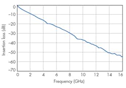
At frequencies beyond several hundred megahertz, dielectric losses in the PCB material or cable insulation dominate attenuation. Signal attenuation or insertion loss can be as high as 30 dB or more in some longer paths. Such attenuation and distortion increase BER. As an example, Fig. 2 shows the insertion-loss frequency-response curve for a two-foot-long stripline transmission line on an FR4 PCB. At 12 GHz, the loss is a staggering 42 dB.
Correcting Signal Degradation
To compensate for signal impairment, one can apply a technique called equalization. Equalization is the process of correcting for the frequency response of the data path. Equalizers are essentially filters that reverse the effects of the transmission channel, meaning that they flatten the frequency response of the path.
Equalization is used at either the transmitter (TX) or the receiver (RX), or both. Fig. 3 shows a signal path that includes both. The TX equalizer, called a feedforward equalizer (FFE), is essentially a high-pass filter that pre-distorts the signal in a way to overcome the degradation of the channel. It boosts the signal level at the rise and fall transitions to compensate for the rounding and signal stretching. While transmitter equalization can be accomplished with an analog filter, most equalization these days is of the digital variety.
The differential data path along the transmission line picks up noise but because of the common-mode rejection properties of a differential pair it is mostly cancelled out. At the receiver the continuous-time linear equalizer (CTLE) and the decision feedback equalizer (DFE) further compensate for the maladies of the transmission path before clock and data recovery (CDR).
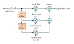
An example of a TX equalizer is a feedforward-equalization (FFE) circuit that’s usually implemented as a finite-impulse-response (FIR) filter (Fig. 4). The delays are one bit time or one UI. The values of the coefficients (cursors) determine the degree of preemphasis. These coefficients are initial estimates, as the actual degree of distortion in the signal path is not known. However, if the coefficients can be readjusted later on, it’s possible to optimize the preemphasis when the channel characteristics are known. Too little or too much equalization can increase ISI and BER.
The coefficients values in Fig. 4 are referred to as cursors. The main cursor is the voltage at the center of a bit. A pre-cursor is the voltage at the center of the bit occurring before the main bit. A post-cursor is the voltage at the center of the bit after the main bit. The output is the sum of the products of the voltages of bits occurring prior to the bit of interest. This form of correction involves emphasizing the voltage transitions and de-emphasizing the non-transitions.
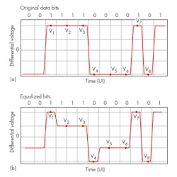
Figure 5 shows the result of equalization on a bit stream. Fig. 5a shows the original unequalized signal; note that each bit voltage is numbered. Fig. 5b is the equalized signal, which is equivalent to a high-pass response that offsets the low-pass response of the data path.
Equalization is also used at the receiver (RX). The two most common types of RX equalization are continuous-time linear equalization (CTLE) and decision-feedback equalization (DFE). A FFE FIR filter can be used at the receiver; the channel response makes it possible to predict the coefficients, allowing for adaptive equalization. A more common arrangement is to use the CTLE and DFE.
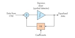
The CTLE is usually a high-gain active RC filter that produces more gain at the higher frequencies to offset the losses in the channel. The DFE uses a FIR like the FFE (Fig. 4, again) in a feedback path as illustrated in Fig. 6. The feedback is the previously detected signal, and it’s subtracted from the incoming signal in an effort to cancel any ISI.
Many devices incorporating high-speed serial interfaces include some form of equalization. However, it can also be added externally as needed by a design. Typical of ICs currently available are Texas Instruments’ DS280BR810 and DS250DF810. The DS280BR810 is a low-power, 28-Gb/s, eight-channel repeater that includes a form of linear equalization. It’s ideal for use on backplanes to extend the reach of ASICs or FPGAs. The DS250BR810 is a 25-Gb/s, eight-channel retimer that’s used to extend the range of signals on backplanes and in fiber-optic equipment. The receivers include an active CTLE and an adaptive DFE; the transmitter includes an FIR filter. A wide range of other devices are available.
Green Box Testing
The key to optimum signal integrity and minimal BER is proper setting of the transmitter FIR coefficients. The TX doesn’t know the characteristics of the channel, so the settings will initially not be the best possible. These settings are an issue in any product using multi-gigabit serial links such as routers, switches, and security equipment.
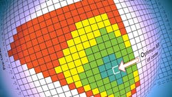
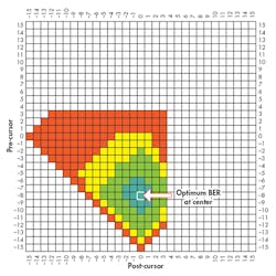
The approach taken by Green Box (GB) testing is to sweep the coefficients over a range and make measurements to establish a pattern that will indicate when the channel is optimized. The outcome is a graphical plot of BER for each pair of TX coefficient settings. The outputs with no errors are colored green. Readings with errors but less than the RX can record are colored yellow, while maximum errors are recorded as red. Fig. 7 shows a typical GB plot.
The basic test procedure is to connect the transmitter to a pseudorandom-binary-sequence (PRBS) generator set to a bit pattern typical of what’s mandated by the interface protocol. Set some initial values for the FIR coefficients—these are the pre-cursor and post-cursor values. Next, transmit the data. Allow several seconds for the RX equalizer to adapt. Then measure the BER at the receiver. Compare the measured BER to a target BER for the system. Plot the result. The optimum set of coefficients is usually in the center of the green region.
Green Box testing is often the fastest and most reliable way to pinpoint the transmitter settings that enable the system to meet the design requirements.
About the Author

Lou Frenzel
Technical Contributing Editor
Lou Frenzel is a Contributing Technology Editor for Electronic Design Magazine where he writes articles and the blog Communique and other online material on the wireless, networking, and communications sectors. Lou interviews executives and engineers, attends conferences, and researches multiple areas. Lou has been writing in some capacity for ED since 2000.
Lou has 25+ years experience in the electronics industry as an engineer and manager. He has held VP level positions with Heathkit, McGraw Hill, and has 9 years of college teaching experience. Lou holds a bachelor’s degree from the University of Houston and a master’s degree from the University of Maryland. He is author of 28 books on computer and electronic subjects and lives in Bulverde, TX with his wife Joan. His website is www.loufrenzel.com.
