Quiet Down To Meet FCC Emissions Standards

Most designers don’t think about the noise they’re creating in the electronics they design. If you’re designing anything with a clock, anything digital, any switching power supply, or anything using a motor, you will radiate electromagnetic interference (EMI) and be held accountable for it before you can get it out the door.
Pretty much all electronics must meet certain minimized noise standards defined by the Federal Communications Commission (FCC). The details are provided in the code of federal regulations, title 47, part 15, subpart B, which outlines the requirements for “unintentional” radiators.
Related Articles
- Simple Grounding Rules Yield Huge Rewards
- Protect Your Fortress From ESD
- Noise Reduction Is Crucial To Mixed-Signal ASIC Design Success
The reason I say most designers don’t think of emissions from their design is because of the plethora of molded-on ferrite beads that we all see on power supply lines coming out of our electronic gadgets. The dreaded ferrite bead on the cable can be avoided, and it is a clear indicator that the design ran into problems trying to clear emissions testing and a quick duct-tape fix was applied in the final hours.
It’s always cheaper to fix the original design than to apply patches after the electronics and mechanics are finalized. Worse yet are field recalls due to your product interfering with the functionality of other devices out there. It’s expensive for instrumentation-type products and the death knell for consumer devices.
This file type includes high resolution graphics and schematics.
This discussion focuses on emissions and EMI from a device, not “signal integrity” issues in a design. Most EMI issues are dealt with at the board and system levels, although some specific techniques can help at the chip level also. My attempt here is to outline a strategy where the methods used cover the most common electronic designs.
Consequently, let’s start with the premise that you’re designing a circuit board in a box with some wires coming out of it. That covers most things that EEs create. We then need a circuit board that serves as a low-impedance ground point at all frequencies. Consequently, we start this process with a high-frequency (HF) grounding strategy (see “Simple Grounding Rules Yields Huge Rewards”). Get the grounding right and we can work from there to make the system quiet enough to keep the FCC happy.
What Are The Sources?
EMI tends to be a multisource problem. Generally when you look at the emissions from a device, you will see multiple sources at distinctly different frequencies. Sometimes reducing the loudest sources is enough to get a product through EMI testing, but frequently you need to make an effort to reduce multiple radiators at different frequencies.
First, identify the unintentional radiators in your design. Digital clocking, switching power supplies, motor drivers (especially arcing brushed motors), and items with repetitive current pumping all are potential EMI sources. Repetitive signals that switch current around will generally be seen in an emissions test analysis.
The important thing is to reduce the magnitude of those repetitive radiators. Intermittent burst noise may also be an issue, and dealing with these sources uses similar techniques. Recognizing the noise generators in the design phase and mitigating potential problems is cheaper than fabricating your design, failing emissions testing, and re-spinning the design.
Circuit Strategy
Once you have a good feel for your noise generators, determine where you can reduce their power or limit their higher harmonic content. If the signal is used in a low-bandwidth path, you really don’t need picosecond rise times and perfect square waves. I/O drivers need to be powerful enough to get the job done, but a clock with significant ninth harmonic content and above is probably beyond what’s needed. An added bonus here is that it generally drops your overall power consumption as well.
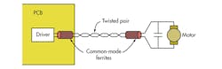
EMI from motors and their wiring, especially dc motors that use armature brushes, presents several different issues. First, the arcing of a brushed armature dc motor makes for a great spark-gap transmitter. Second, varying the duty cycle of the power supplied often controls motor speed, and that motor commutation causes back electromotive force (EMF) voltage spikes on the motor winding since the current is shut off in an inductor. Finally, the wires between the printed-circuit board (PCB) and the motor serve as an antenna for both the common-mode noise generated at the PCB and the noise generated by the motor itself.
The circuit requires a small amount of capacitance at the motor for arcing (typically 100 pf to 0.1 µF for small motors), a common-mode choke on the connection leaving the PCB for the motor, and another ferrite at the motor itself. The circuit will probably need a flyback diode or a snubber circuit on the motor to protect the driver transistors (Fig. 1).
Physical PCB Strategy
An antenna designer will talk about quarter-wave radiators as your basic antenna. For an emissions problem, it’s generally a collection of inefficient antennas that are often much smaller than the ideal quarter wavelength. As an example, if you have a square-wave 100-MHz signal, there will be significant energy in the third and fifth harmonics. The quarter wavelength for the fundamental is 28 inches, but the fifth harmonic is 5.6 inches. For that example, don’t be surprised to get emissions from connections that are at one-twentieth of a wavelength, so a conductor only an inch long will be a radiator in this example.
The bottom line is to reduce your onboard antenna size wherever possible. Keep it short, or try to enclose it between ground planes if it has a lot of switching noise. On-board layers with signals using flooded ground planes around signal lines will help with both EMI and signal integrity on the board.
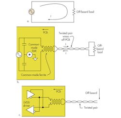
One of the biggest offenders here is the popular use of switching power supplies. Although they are very efficient, their driver circuits can be very noisy. Minimize the connection size associated with the driver side of the LC section of these devices (Fig. 2).

Connections Outside
Wires off the board can become some of the strongest radiators due to long length, but are generally easy to control. We can lump these wires into a few categories: power, grounds, shields, ground referenced signals, and differential signals.
Ground referenced signals going down a wire don’t tend to be very well ground referenced, so to speak. If you’re trying to maintain anything with good value integrity, the impedance of the wire tends to be a source of problems. Thankfully, most modern designs have had their learning experiences and lack such connections. Most modern systems use differential signals for both analog signals and digital data communication. In both cases, the use of twisted-pair wires creates a tight common-mode characteristic between the two wires, which is useful.
The differential data paths used with high-speed serial links such as USB and Ethernet benefit from common-mode chokes inserted at each end of the twisted-pair wires. This has a double benefit. The common-mode EMI present on the PCB does not make it onto the wires, and common-mode signals due to the ground bounce between the devices at both ends of the cable get attenuated. Common-mode chokes are available for industry-standard low-voltage differential signal (LVDS) devices.
The use of the twisted-pair wires off board for all your connections also helps avoid the creation of a loop antenna. If you have an open loop of wire, the current in that loop creates a field. If the current in the wire going out is tightly placed with the current in the wire returning, superposition of the two fields mostly cancels and minimizes radiation (Fig. 3).
The twisted pair doesn’t help with common-mode radiation from the wires, where both wires are radiating the same signal. The noise is picked up by both wires, not just one, and you have a driven antenna that needs a common-mode choke to silence it. The common-mode problem also happens with a shielded wire, and the shield functions as the radiator.
Power connections need to be fitted with a common-mode ferrite choke, where both wires go through the same ferrite body. By doing this, the average dc currents cancel with minimal magnetic field created in the ferrite. Signals common to both wires, namely EMI, get magnetically coupled and thus impeded. This choke should be built onto the PCB at the enclosure exit. The industry term for this device is a “current compensated power line filter,” and it’s done as two wires wound on the same ferrite core in the same direction.
Shield Box
Do you need to put your design in a metal shield box? Hopefully with the steps outlined here, the answer is no. But for large designs with lots of noise sources, you should be prepared to do so. Most consumer products end up in a plastic enclosure, so you can prepare for a lower-cost alternative, using a conductive coating inside the case.
Consequently, when your mechanical team is designing the enclosure, be sure to have the conversation on how to build a Faraday cage and be prepared to add a conductive internal coating. Any opening through the box needs to be considered an EMI port.
Advanced Techniques
These methods will take care of most common electronics products. Some special techniques are available where the noise generator is especially “loud” or where the environment is especially sensitive to radiated noise.
The common clock in computer systems generally results in a single-frequency EMI spike at the clock fundamental (plus harmonics). After that clock has been distributed and used throughout the system, the EMI power at that one frequency can be significant. The use of spectral spreading takes that one frequency and adds some variance to it. The variance or “frequency dithering” results in a clock in which the amplitude of the radiated emissions is lower, while having a wider bandwidth (Fig. 4).

Everyone who has ever torn down a cell phone has seen examples of localized shield cans used over select parts of the PCB for isolation. The technique works well, as long as the shield can is carefully matched with a ground plane as part of the PCB. Except for specialized situations, this approach is generally not needed to meet emissions requirements.
Conclusion
If you make an effort to reduce your noise sources, do a careful board layout that controls your PCB antennas, and choke all your external antenna wires, many devices will clear FCC emissions testing without a shield box. If nothing else, these practices should reduce emissions driven redesigns and eliminate that ugly ferrite molded into the power cable.
Jerry Twomey has been involved in IC and PCB design since 1979. He has designed multiple consumer, commercial, and medical products including data communication, satellite systems, video, medical instrumentation, disk drives, cell phones, RF transmitters and receivers, and many others. Mixed-signal systems and design are his primary focus with a special interest in things not easily defined or solved. In addition to design, he teaches in both industry and academia and is a Senior Member of the IEEE. He holds an MSEE from Worcester Polytechnic Institute. He can be reached at [email protected].
This file type includes high resolution graphics and schematics.
About the Author

Jerry Twomey
Founder and Engineering Consultant, Effective Electrons
Jerry Twomey has extensive experience designing electronics for medical devices, electromechanical systems, and transistor-level integrated circuits. This includes many consumer, medical, aerospace, and commercial products.
Jerry holds several patents and is an author of multiple trade magazine publications, many of which appeared in Electronic Design magazine, providing solutions for commonly encountered design problems. He teaches seminars in embedded systems, IC design, EMC, and medical technology, and has lectured at UCSD. Jerry has also chaired the San Diego IEEE chapters for Microwaves and for Solid State Circuits.
Jerry Twomey is the author of Applied Embedded Electronics – Design Essentials for Robust Systems, a comprehensive reference book covering the design process for embedded-systems electronics from initial concept to final PCB.
Comment About the Article
To join the conversation, and become an exclusive member of Electronic Design, create an account today!

Leaders relevant to this article: