This file type includes high-resolution graphics and schematics when applicable.
Embedded video-system design for applications such as virtual reality (VR) and augmented reality (AR), mobile, and smart TVs is challenging, in part, because of the interface demands. Higher performance requirements continue to escalate due to the deployment of higher-resolution solutions.
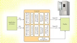
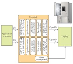
Lattice Semiconductor recently introduced its CrossLink technology (see figure). It’s the first programmable application-specific standard product (pASSP) interface bridge that supports leading protocols for mobile image sensors and displays. I talked with Subra Chandramouli, Director of Marketing for the mobile and consumer division at Lattice Semiconductor, about CrossLink and how it addresses the latest video-system interface challenges.
Wong: What led Lattice to develop CrossLink technology?
Chandramouli: Today’s embedded video-system designers face complex challenges in regard to video input/output interfacing in a climate of constant innovation. Rapid advances in mobile application processors; the proliferation of low-cost image sensors and displays; and the widespread adoption of Mobile Industry Processor Interface (MIPI) standard interfaces have revolutionized embedded-system design in recent years. These mobile platforms are at the core of new technologies in smartphones and tablets, as well as in DSLR cameras, drones, VR and AR systems, medical tools, and industrial displays.
In a perfect world, each device in a system would interface directly to the applications processor. But in today’s ever-evolving video markets, that is often not the case. Engineers frequently find that the interface type or number of interfaces on the applications processor and those on the system’s image sensors or displays do not match up.
Wong: Can you expand on how this challenge can be addressed, and how that solution relates to the CrossLink solution?
Chandramouli: Embedded video designers need high-performance, low-power, and compact interface bridges that can resolve these connectivity problems in a way that maximizes design flexibility and continues to encourage innovation. They need a bridging solution that can convert incompatible interfaces between cameras, displays, and processors; combine multiple video-stream inputs into a single interface output; or split video streams into multiple interfaces. This bridging solution would have to support a broad range of both new and legacy interfaces. Finally, it must deliver a high level of performance without violating strict system power and footprint constraints.
To meet these needs, Lattice Semiconductor developed the CrossLink solution, the first pASSP interface bridge that supports leading protocols for mobile image sensors and displays. The CrossLink device combines the flexibility and fast time-to-market of a FPGA with the power and functional optimization of an ASSP, creating a new product class called pASSP.
As the first solution in this category, CrossLink devices are low-cost video-interface bridges with the highest bandwidth, lowest power consumption, and smallest footprint. It is a solution ideally suited to wide-ranging applications, from VR headsets, drones, and DSLR cameras to smartphones, tablets, and wearable devices.
Wong: How does the CrossLink solution work to address these issues?
Chandramouli: The CrossLink solution is an entirely new breed of bridging devices, engineered with designers’ needs in mind to fit an array of applications and imbued with a comprehensive feature set. The CrossLink solution is the industry’s fastest MIPI D-PHY physical-layer-specification bridging solution supporting speeds up to 12 Gb/s.
To maximize designer flexibility, it supports a wide range of current interfaces and protocols (MIPI D-PHY, MIPI CSI-2 camera interface specification, MIPI Display Serial Interface (DSI) among them). It also supports many legacy video interfaces and protocols such as CMOS, RGB, MIPI DPI, MIPI DBI, SubLVDS, SLVS, LVDS, and OpenLDI.
But we also kept the demands of consumer applications in mind during CrossLink’s development. For this reason, it features a low operating power of less than 100 mW for many use cases. CrossLink is also the first programmable bridging solution with a sleep mode and is compact enough to fit into a footprint as small as 6 mm2.
To deliver fully customizable interfacing solutions, the CrossLink solution includes a mobile FPGA fabric with multiple physical interfaces. Each CrossLink IC features up to two embedded MIPI D-PHY blocks, with each block containing up to four data lanes and a clock to support transmit and receive functions. The adjacent FPGA fabric integrates 5,936 LUTs, 180 kb of block RAM, and 47 kb of distributed RAM.
The functions that these FPGA resources can support are incredibly diverse, and include multiplexing, merging, de-multiplexing, arbitrating, splitting, data conversion, and custom protocol design. Data rates range up to 1.5 Gb/s/lane using two hard D-PHYs and up to 1.2 Gb/s/lane using programmable differential I/O blocks. Finally, the CrossLink device adds 15 programmable differential IOs, extensive GPIO resources, 10-kHz and 48-MHz oscillators and PLLs, two user I2C embedded blocks for system functions, as well as I2C/SPI device configuration.
Wong: What would be some typical applications for the CrossLink solution?
Chandramouli: There are many new and exciting applications for this market in consumer and industrial applications.
In consumer applications, such as gesture recognition for gaming or accident avoidance for drones, a camera aggregator is needed to serve as a hub to manage multiple MIPI CSI-2 image sensors. In these applications designers may need to merge multiple image-sensor inputs into a single larger frame, multiplex between image sensors, or arbitrate between image sensors based on virtual channels.
For example, to create a depth perception in an AR system, a bridge must merge multiple MIPI CSI-2 camera inputs into a larger single-frame output with minimal frames captured at the same moment in time. The CrossLink solution allows designers to interface to multiple MIPI CSI-2 image sensors simultaneously, capturing each image sensor in synchronicity and with minimal latency.
In the industrial settings, such as surveillance cameras and machine-vision systems, designers need to bridge between high-end image sensors and mobile application processors. Many of the image sensors in these applications offer excellent performance, but use a proprietary interface originally developed by the sensor manufacturer.
To leverage the innovations available on popular mobile application processors, designers building embedded applications must convert the signal from those proprietary image sensor interfaces to a mobile MIPI CSI-2 image sensor interface found on most of today’s mobile application processors. Using its programmable fabric, the CrossLink device lets developers build compact, high-performance, low-power interface bridges that can convert a signal from those proprietary interfaces to MIPI CSI-2.
Looking for parts? Go to SourceESB.
This file type includes high-resolution graphics and schematics when applicable.


