Commercial curve tracers have existed for decades. But designers without access to one can create a simple circuit that uses a function generator and oscilloscope to generate JFET transfer and characteristic curves. The circuit can also be computer-driven, with software displaying and recording the curves.
Using these curves, designers can match devices, determine their transconductance and output resistance, and accurately bias JFET-based amplifiers. These curves are also valuable because JFET characteristics vary widely within a specific part number due to manufacturing variability and because data sheets may show any combination of typical curves, a variety of possible curves, or no curves at all.
The circuit generates two curves that describe JFET behavior. The transfer curve plots drain-source current (IDS) versus gate-source voltage (VGS) with a fixed drain-source voltage (VDS), and the characteristic curve plots IDS versus VDS with VGS fixed.
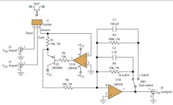
The circuit is a simple transimpedance amplifier that converts the device under test’s (DUT’s) IDS into an output voltage (Fig. 1). Op-amp U1A maintains the DUT’s source voltage at 0 V. It does this by drawing the DUT’s IDS through R1. As that IDS flows through R1, it creates a negative voltage at Q1’s emitter equal to (IDS)(R1). Op-amp U1B inverts this voltage and buffers it out for plotting, scaled at either 1 mA or 10 mA per volt.
Fig 1. The curve tracer circuit is a simple transimpedance amplifier that converts the device test's IDS into an output voltage.
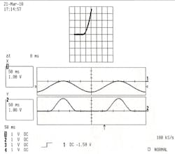
Figure 2 is an oscilloscope screenshot of a transfer curve being generated for a 2N5457 n-channel JFET. The lower half shows standard voltage-versus-time plots, and the upper half is an XY plot of the same data. The upper trace (channel 1) is VGS, a sine wave varying between 0 and –2.5 V, coming from a function generator.
Fig 2. This example of results for a 2N5457 n-channel JFET shows an XY plot of the device's transfer curve (top). The curve is based on the data in the voltage-versus-time plots of VGS (channel 1) and IDS (channel 2). In this example, VDS was held at 15 V.
The circuit output voltage is proportional to IDS (channel 2, lower trace), which varies from 0 to 3 mA. In this case, VDS is being held at 15 V. The XY plot represents the JFET’s transfer curve, and IDSS and VGS (off) can be determined to be 3 mA and –1.25 V, respectively.
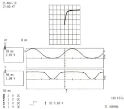
The oscilloscope plot in Figure 3 shows a characteristic curve being generated for the same JFET. VDS (channel 1, upper trace) is a 0- to 8-V sinusoid from the function generator. The JFET’s IDS (channel 2, lower trace) varies from 0 to 3 mA. In this case, VGS is being held at 0 V.
Fig 3. These results show the other JFET curve, the characteristic curve. Scope channel 1 shows VDS and channel 2 shows IDS. In this case, VGS was held at 0 V.
Figure 3’s XY plot represents one of the JFET’s characteristic curves. The corner voltage (where the curve transitions from almost linear to almost flat) is the transistor’s pinch-off voltage, VPO, which is equal to the negative of VGS (off). The slope of the “almost flat” portion of the curve is the inverse of the JFET’s output resistance.
The region to the left of VPO is called the ohmic region (where the JFET can be used as a variable resistor). To the right of VPO, the JFET operates in “saturation,” with VGS controlling the drain-source current. A family of characteristic curves can be generated by varying VGS from 0 V down to VGS (off), which is –1.25 V for this device.
If you’re only testing n-channel JFETs, a Schottky diode can be installed from the VDS input to ground, preventing inadvertent forward biasing of the JFET’s gate.


