
Verification solutions must be usable across the complete flow, from block-level verification to full system-on-chip (SoC) simulation. Graph-based solutions can meet this requirement (see “Sizing Up The Verification Problem”). However, that’s just one aspect of a verification solution’s scalability. Most companies use a bottom-up flow, which has some implications on the tools that they use for verification. Some companies, though, are moving to a top-down flow because today’s systems involve more than hardware.
Related Articles
- Sizing Up The Verification Problem
- Faster JESD204B Standard Presents Verification Challenges
- Hybrid Execution And Software-Driven Verification Will Emerge In 2013
Traditional Verification
Most companies use bottom-up verification simply because of historical reasons. Until recently, the implementation model was the only executable model that existed for the system. That description was written at the register transfer level (RTL), and it is considered to be the golden model for the design. This was the first point at which any form of verification could begin.
The development process then follows the traditional V diagram where verification forms the right edge of the V (Fig. 1). On the left side of the V, the design was decomposed from a paper specification, often an iterative process, and it might have included the selection of intellectual property (IP) blocks and formation of the chip architecture. Aspects of the system such as the communications network were also defined at this stage.
This file type includes high resolution graphics and schematics.
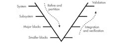
The process stopped when the blocks defined were small enough for a single engineer or a small group of engineers to implement. Specifications for the blocks were still defined in paper documents. Individual blocks were verified, integrated into subsystems, and re-verified. That process was repeated all the way until the full system had been assembled. At that point, some level of validation of the full SoC specification could also be attempted.
This process is failing for a number of reasons, including the speed of software simulators when full chips are assembled and the difficulty in creating useful tests at the system level using constrained-random generation tools. Also, none of these tools can test things other than pure functionality.
For example, a constrained-random approach can’t develop a stress test or a test for measuring performance. Emulation and FPGA prototyping can be used to improve the performance of the simulation process. However, these approaches require significant changes in the testbench or even a change in verification methodology. In addition, they trade off performance for other aspects such as cost, turnaround time, visibility, and debuggability. Simulation, emulation, and prototyping are each superior solutions at some point in the verification flow, so many companies are now employing all three in their methodology.
Processors Complicate The Process
Another significant difficulty comes with designs that include one or more processors, and there are few SoCs these days that don’t. In fact, the vast majority of complex chips have several heterogeneous processors. The constrained-random process requires these processors to be removed and replaced by a transactor model. Stimulus is then generated by the tool and fed into the transactor to emulate operations on the processor bus. The tool has to take this approach because it has no way to generate software to run on the processors. Running production code, even if it is ready, may constrain the verification process too much.
This replacement provides fine control over the busses, although it may be difficult to constrain it to realistic sequences, as would be generated by a processor. Processor removal makes the transition to emulation and FPGA prototypes difficult because this separation would create a significant amount of traffic between the hardware-accelerated portion of the design and the portion of the design that remains in a software simulator, including the testbench. The communication would reduce the performance of the hardware portion. In addition, having different strategies for the processors would again require a change in verification methodology. A consistent verification methodology is a second dimension of scalability that existing solutions don’t address.
Changing Methodology
This bottom-up verification methodology is breaking down rapidly, and many of the most advanced semiconductor companies are now switching to a top-down flow principally because systems are no longer just about the hardware. Today, the differentiation in systems comes from the software. Due to tightening product development cycles, the software team cannot wait until completion of the hardware implementation to start software integration and verification.
In many cases, design decisions need to be made by both teams working together. This requires an executable model much earlier in the design process, a model generally called a virtual prototype. These virtual prototypes are written at the transaction level using languages such as C, C++, or SystemC. Models do not contain all of the implementation detail and can execute much faster than RTL models.
This file type includes high resolution graphics and schematics.
In many cases, models are fast enough to be able to execute significant amounts of software. The lack of implementation detail means that these models cannot be the only ones on which verification is performed. Changes in timing, even slight changes, can affect the way in which the system operates. Good design practices can minimize this impact.
In terms of the V diagram, we are starting to perform verification on the left edge of the V as design decisions are made. This is not a problem. It is an opportunity because, when verification starts earlier, many important aspects of a system can be verified before time is spent on the detailed design. This, in turn, means that specifications for the blocks are pre-verified. While it would be premature to say that integration problems are a thing of the past, a verified specification will prevent this type of problem from being found late in the design cycle.
Bringing Formal Verification Into The Picture
While simulation is used for a significant portion of the verification process, formal verification can perform some tasks faster and more completely than simulation. This is especially true when a system includes safety-critical functionality or high-risk parts of the design. This may include the communications infrastructure or those aspects of a system involved with data integrity. Until now, it has been difficult to effectively combine formal verification with simulation and to be able to define them in a way that limits overlap and repetition in the verification process. This inability inevitably leads to wasted time and resources.
Standards such as the recently announced Accellera Universal Coverage Interoperability Standard (UCIS) hope to find ways to reduce this redundancy, but coverage metrics used by the two methodologies are based on different concepts and combining them is difficult. Formal methods use a response-based metric system, whereas constrained-random methods use a stimulus-based metric.
A unified metric is the ideal approach. Given that stimulus-based coverage associated with the constrained-random process has problems related to actual effectiveness of the verification process,1 a metric similar to those used by formal verification based on goals or outcomes would be better. Also, the transformation of verification goals to the stimulus metrics in use today is one of the most difficult tasks in the methodology.2
Scalability In A Top-Down Flow
A verification methodology that can evolve throughout the design and implementation flow and bring formal methods and simulation closer together is needed. It must be able to work with the virtual prototype and RTL model executed by a simulator, emulator, or FPGA prototype. A single testbench should be able to work with all of these elements during the development flow.
This also brings about some other requirements for the verification methodology. For example, it should be possible to start verification with a partial testbench because we cannot have the entire process stalled waiting for a single piece. Over time, the testbench can be refined along with the design. It should be possible to verify at the complete system level, the block level, and everything in between with the fewest changes possible. However, the bottom-up aspect of the flow does not go away, especially when IP blocks are to be used within the system.
The testbench created for IP blocks should be consumable by the higher levels of integration without change or the need to be able to understand them. We have thus defined three fundamental scalability needs of a solution within a flow:
• It should work across all abstractions.
• It should work with all methods of model execution.
• It should integrate formal verification into the flow.
Verification From The Inside Out
The key aspect to making a flow such as this possible is to focus on the processors, designed, along with the communications infrastructure, to be able to control other aspects of the chip. Rather than seeing processor buses as primary inputs to the design that have to be controlled by a constrained-random pattern generator, it is better to write software that will run on those processors to perform the necessary verification. A simulator, emulator, FPGA prototype, or even the final chip should all be able to run the same software. The same is true for the virtual prototype so long as the processor model is source-code compatible. Most models go much further than this and are object-code compatible with the actual device.
But writing software manually is not the solution, equivalent to creating directed tests for other pieces of the design. Instead, the software should be automatically generated, with each software test case verifying a particular aspect of the design, which is key. We do not want to generate random test cases with the hope that it will do something useful and then spend time and effort looking for the ones that do. Rather, we want each test to be created for a defined purpose to satisfy a particular coverage goal.
How does all of this happen? The graph-based model is a fundamental part of the solution. If SoC functionality is represented as a graph-based scenario model, verification goals are shown on the left with design inputs on the right (Fig. 2). Constrained-random stimulus starts at the right and attempts to reach interesting verification states with no guarantee of success.
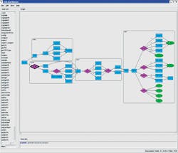
In contrast, a graph-based constraint solver can select a verification goal, determine exactly the path needed to achieve that goal, and generate the appropriate software test case to execute on the embedded processors. As an added benefit, this goal-based verification approach is more aligned with formal verification, making it easier to consider a single, unified, verification methodology.
Conclusions
Scalability is necessary for a modern verification flow, including the ability to consistently use different execution engines such as a virtual prototype, simulator, emulator, or FPGA prototype. The verification methodology must be able to handle multiple levels of abstraction so the same approach can be used throughout the development process.
Unifying formal verification into the flow would eliminate unnecessary verification. Graph-based verification with a solver based on goal satisfaction can generate software to run on the processors and coordinate that with external stimulus to produce highly efficient verification test cases.
References
1. Mark Hampton, “Functional Qualification,” EE Times EDA Designline, www.eetimes.com/design/eda-design/4018490/Functional-Qualification
2. Brian Bailey, “DVCon Panel: Verification planning,” EDN, www.edn.com/electronics-blogs/practical-chip-design/4408522/DVCon-Panel--Verification-planning
Adnan Hamid is cofounder and CEO of Breker Verification Systems. Prior to starting Breker in 2003, he worked at AMD as department manager of the System Logic Division. Previously, he served as a member of the consulting staff at AMD and Cadence Design Systems. He graduated from Princeton University with bachelor of science degrees in electrical engineering and computer science and holds an MBA from the McCombs School of Business at the University of Texas.
This file type includes high resolution graphics and schematics.
About the Author
Adnan Hamid
CEO
Adnan Hamid is the founder and chief executive officer of Breker Verification Systems, and inventor of its core technology. He has more than 20 years of experience in functional verification automation and is a pioneer in bringing to market the first commercially available solution for Portable Stimulus. Prior to Breker, Hamid managed AMD’s System Logic Division and led its verification group to create the first test case generator providing 100% coverage for an x86-class microprocessor. Hamid holds 12 patents in test case generation and synthesis. He received Bachelor of Science degrees in Electrical Engineering and Computer Science from Princeton University, and an MBA from the University of Texas at Austin.
Comment About the Article
To join the conversation, and become an exclusive member of Electronic Design, create an account today!

Leaders relevant to this article: