The number one thing engineers care about these days is time-to-market, or more aptly put, time-to-revenue. After all, companies are in business not to develop technology, but to make and sell products based on that technology. To compete in today’s fast-paced global market, though, engineers have to design their products faster and better. They have to get them right the first time and to market ahead of the competition, without sacrificing reliability or performance.
Related Articles
- What's The Difference Between Ad Hoc And Formal Version Control
- Data Management For EDA Apps Sees Gains In 2011
- Unified Graphical System Design Environments Boost Design Success Rates
Time-to-market targets are no longer optional. But product release dates are rarely met, if ever. Virtually any designer these days will readily acknowledge that. A few designers may say they meet their target release dates, but dig a little deeper and you’ll discover that the dates were changed or, worse yet, important product features and functions were removed.
Meeting those all too elusive release dates means addressing the core reason for design delays in the first place—the design process created by the traditional design tool chain. The ideal solution is the use of a unified design environment. Whether or not engineers opt to utilize this approach will directly impact their ability to meet product release date targets and, ultimately, shorten their time-to-revenue.
Traditional Tool Chain Approach
The age old approach to designing electronic products consists of many individual pieces with design domains and/or individual designers existing in their own design silos. This “tool chain” perpetuates a scenario in which the schematic designer uses a tool from one vendor, the printed-circuit board (PCB) designer uses a tool from another vendor, and the libraries are managed using a tool from a different vendor altogether (Fig. 1). This scenario plays out in every stage of the design process and results in potentially 10 to 15 separate tool packages being purchased and used just to release a product. Understandably, tremendous bottlenecks occur in the interconnections or processes between these tools.
EDA vendors worked to resolve these bottlenecks by developing “integrated suites,” which seamlessly integrate various tools together in one package. But even when a tool is marked as having come from a vendor selling an integrated suite, chances are it actually came from another vendor and was simply banded together with yet other vendors’ products and sold as one solution. At its core, the integrated suite is still just a collection of individual products from different companies.
But why does this approach make it difficult for engineers to meet their product release dates? The problem isn’t that the solutions don’t allow engineers to properly draw a schematic or create a PCB, for example. They do that just fine. The problem occurs when engineers make design changes. How do they make, propagate, and, most importantly, document those changes? With the standard tool chain, there is no good answer, and that’s the crux of the issue.
Engineers spend a good portion of each day—by some accounts 40% to 60%—processing, communicating, and disseminating information within the manual, translation-laden design process. That’s time the engineer should be using to invent the next cool feature or product and to hit a product’s release date.
Instead, these integrated tool suites and the traditional tool chain hold back productivity. That’s because they involve a great deal of iteration, make it difficult to keep design elements in sync with one another, bog designers down with data integrity issues, and follow disjointed flows. In other words, when engineers don’t make their release dates, it’s always because of some process-oriented reason.
Finding an alternate option to the integrated tool suite and the traditional tool chain design approach is absolutely essential to engineers who must now design their products faster and better to maintain a competitive edge.
Unified Design Environment
The single biggest opportunity for speeding the design process from concept to manufacture and achieving those all too elusive product release dates lies in increasing productivity within the design tool chain. By improving productivity, engineers save time—enabling them to focus on their core area of engineering competency rather than the process itself—while also gaining design fidelity and reliability. A unified, streamlined design approach offers the ideal way to achieve this goal.
With a unified design approach, the design progresses from concept to manufacture in a single, unified electronics design environment. Rather than a collection of individual products banded together in an integrated tool suite, it relies on a single unified tool that offers all expected design process functionality (e.g., the ability to draw a schematic or create a PCB), plus all process-oriented capabilities that traditionally bog engineers down (e.g., netlists, e-mail chains, spreadsheets, and sticky notes). Using the unified design environment, engineers can make, propagate, and document design changes throughout the entire design process with the simple push of a button.
The unified design environment includes several key features:
• Native version control ensures that all of the traditional paperwork-oriented processes that engineers are familiar with such as release and library management are native to the engineering desktop.
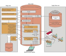
• Relational databases, implemented as server-based software applications, store and manage electronic design data. The databases allow formal revisions and life-cycle management of components and data used in a design. They also provide intelligent links to the supply chain to give real-time information about the parts specified in a design and provide a mechanism to easily and securely share design data (Fig. 2).
• All the elements in a design can be synchronized. For example, a schematic can be synchronized to a PCB design as well as to a bill of materials.
• The intuitive and graphical user interface is extremely powerful, yet also quick and easy to learn.
With these features, engineers gain access to excellent data management, which enables them to quickly and easily access the data they want, when they want it. Engineers then can make faster, better designs to reduce time-to-revenue and eliminate missed or repeated processes, all while reducing errors in design, purchasing, and manufacturing. The data is clear, accurate, and reliable, encouraging design reuse at both the component and circuit level. The ability to reuse parts or all of an entire design saves a tremendous amount of time.
Conclusion
Meeting time-to-market or time-to-revenue targets is critical for engineers who want to maintain a competitive edge in today’s fast paced electronics industry. Achieving those targets requires a design approach that addresses the core reason behind time delays in the traditional tool chain—the process itself. Today’s manual, multiple file format, translation-laden, status quo tools offer little hope in overcoming the process-oriented issues that continually eat away at the engineer’s time and make release dates a moving target. Integrated tool suites, with their collection of individual tools banded together, also fail to address these issues.
Faced with this stark reality, engineers must seek out an alternate solution. By directly addressing the process-oriented problems associated with the traditional design approach, the unified design environment increases engineering productivity and frees engineers to do what they do best—design. In doing so, it enables engineers to make better designs to reduce time-to-revenue and makes achieving product release dates a reality.
Lawrence Romine is a business development manager at Altium. He has 14 years of experience in the electronics industry, first as an electrical engineer designing high-end audio amplifiers for the audiophile market space and then moving to sales and support of FPGAs for five years. Following his time in the semiconductor industry, he moved to the EDA industry, where he has held various positions with Altium Inc. including sales, support, business development, and marketing.


