Pattern matching is best known for its use in detecting lithographic hotspots, but it’s also widely used across all physical verification flows, and has expanded into design-for-manufacturing (DFM) flows as well. Integrating pattern-matching functionality into DFM operations ensures that designs are quickly and accurately optimized for reliability, performance, and manufacturing prior to tapeout. Combining pattern matching with DFM vector profiles has a wide range of uses in design enhancement, including:
- Automatically finding illegal metal patterns and device/shape orientations as part of the physical-verification flow.
- Ensuring compliance with symmetry and matching requirements.
- Providing context-aware checks for device orientation, symmetry, and matching requirements, as well as other reliability, DFM, and yield requirements.
- Improving fill turnaround time and consistency, especially for analog applications.
- Enabling layout analysis with exact and partial matches to find lithographic/process hotspots earlier in the design flow, and improve future scoring for hotspot pattern libraries based on area of mismatch.
How does it work? In DFM processes, metadata associated with layout objects (such as polygons, edges, and errors) is used to calculate DFM scores and filter data. This metadata (known as a DFM property) can be a numeric, string, or vector property, and each DFM property has a name and a value. DFM properties are different from layout properties (e.g., area, aspect ratio, etc.) and database properties (such as net names), which are attributes stored on geometries in the original layout database.
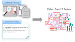
Pattern matching is divided into two stages: capture and match. In the capture stage, designers select areas of interest, using either graphical selection or pattern capture commands (see figure). Designers also have the flexibility to define patterns based on marker layers or hotspot geometries, and to define allowed variations, such as orientations, halo size, etc. Input to the pattern-matching process can be filtered by selecting locations and polygons with certain DFM properties.
Patterns can be captured graphically or by using pattern capture commands.
In the matching stage, the derived layers (pre-filtered) are passed as input, and the matched locations undergo post-processing by inspecting and stamping the output with various properties that allow for more capabilities and applications. These output properties, which contain pattern information such as the pattern ID (PID) and pattern orientations, can either be built-in properties containing pattern information, or extended to embed user-defined properties for more custom processing.
Combining Pattern Matching with DFM Properties
Pattern matching can integrate with a variety of DFM property types to produce multiple applications to ensure design optimization. Three of the most typical uses include:
String/numeric built-in pattern properties
- Orientation checking: This flow is used to analyze and validate legal metal/device orientation, and to check for orientation uniformity and consistency in electrostatic-discharge (ESD) protection structures.
- Orientation-aware fill: A pattern-based, orientation-aware fill flow allows for consistent handling of similar patterns by doing classification and handling for unique patterns before back-annotating the processing results to all original patterns. This flow is essential for meeting design requirements on both electrical and process sides.
String/numeric user-defined pattern properties
Users can apply equation-based design rule checking (DRC) for actions like partial pattern-match identification, and then use the mismatch percentage to determine if and how the selected geometry should be adjusted to fully match the target pattern.
Vector properties
This flow accumulates all values of a DFM property, and displays all versions of that DFM property that share the same location. This vector information can then be used to perform activities such as pattern-clustering analysis and symmetry analysis:
- Pattern-clustering conditions are located by analyzing the vectors of pattern IDs (PIDs) that match the same location. If two PIDs have the same location and orientation, it’s usually because one PID is a subset of the other.
- Symmetry analysis is performed by using the vector properties to check the orientation of each PID, and then analyzing and reporting the results per layer. Subsequently, pattern matching is used to debug the source of symmetry mismatches.
- Context-aware checks combine geometric pattern matching with topological pattern matching to access a new dimension of checking device and net patterns.
When used in conjunction with DFM vector properties, pattern-matching functionality has a wide range of uses in design enhancement and optimization. Designers who take advantage of this combination can gain strategic market advantage.
Sherif Hany is a Technical Marketing Engineer for Mentor, a Siemens Business.


