How to Design an IoT Smart Sensor with an Ultra-Low-Power MSP430FR MCU

Download this article in PDF format.
The Internet of Things (IoT) is quickly becoming ubiquitous, whether in the home, on the factory floor, or say, at the doctor’s office (Fig. 1). For the system engineer, there are many approaches to architect an IoT system, but a basic design has three layers:
An end node gathers information about a process from a variety of sensors. Typical data includes temperature, pressure, speed, vibration, images, audio, physiological metrics, and much more. The node then sends the information via a wired or wireless link to a gateway layer that aggregates the information from multiple nodes and sends it upstream. Finally, the cloud or enterprise layer processes the data streams to control the operation of the various functions, as well as gathers data to identify longer-term opportunities for process improvement (data analytics).
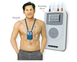
1. A Holter monitor is an IoT smart-sensing application that requires both DSP processing capability and low-power operation. (Source: Mayo Clinic)
End-Node Processing of Computationally Intensive Functions
There are, of course, alternatives to sending all of the data back to the cloud for processing and action. Pushing out processing functions to the gateway or the node—a strategy sometimes called “fog computing”—reduces the load on the network and gives a faster response. For the node, in particular, adding a microcontroller (MCU) can considerably complicate the design. If power-hungry digital-signal-processing (DSP) functions such as finite-impulse-response (FIR) filters and fast Fourier transform (FFT) frequency analysis are a requirement, the challenges proliferate, especially if it’s a battery-powered home or medical IoT application.
The MCU for a computationally-intensive IoT node must perform three main functions:
1. Acquire the data to be processed, which can arrive in either analog or digital format. A pressure sensor, for example, might require an analog front end to buffer and amplify the signal, feeding an analog-to-digital converter (ADC); or the data can arrive via a serial link such as SPI, I2C or UART. The design will be more compact and lower-cost if the MCU includes the analog or digital functions as internal blocks.
2. After the MCU has acquired the data, it applies DSP techniques to extract the desired information. The MCU can accomplish these tasks purely in software, which is slow and takes up large amounts of central-processing-unit (CPU) resources, or with the help of a hardware coprocessor that’s designed to efficiently perform common DSP functions. This is much faster and reduces CPU workload, but often increases power consumption.
3. Once information is extracted, the MCU must take appropriate action. It can take the form of making a decision based on a result from an FFT or FIR, or simply exporting the information via a wired or wireless connection such as I2C, SPI, RS-485, Wi-Fi, Bluetooth, ZigBee, etc. Many options exist, and the MCU must include the appropriate internal blocks even if the physical layer is an external device.
Texas Instruments’ MSP430 family of microcontrollers is optimized for ultra-low-power applications, with multiple low-power modes and power consumption as low as 15 nA (shutdown mode). The MSP430 series is based on a 16-bit RISC core running at up to 16 MHz. The family contains over 500 devices with a rich choice of features including 10-, 12-, or 24-bit ADCs; analog blocks (e.g., op amps and comparators); capacitive touchscreen interfaces; liquid-crystal-display (LCD) drivers; AES encryption; and serial interfaces such as I2C, SPI, and USB.
The MSP430FRxx subset of 109 devices adds ferroelectric random-access-memory (FRAM) technology to the feature set. FRAM is non-volatile like flash memory, but offers fast and low-power writes, a write endurance of 1015 cycles, enhanced code and data security, and high resistance to radiation and electromagnetic fields. The fast write and read speeds make it a good fit for data logging and as a slow-speed RAM to store rarely accessed data.
The MSP430FR5994 device is particularly suited to computationally intensive IoT applications. In addition to 256 kB of FRAM, it includes the Low Energy Accelerator (LEA) module (Fig. 2), a low-power vector math engine that performs signal processing, matrix multiplication, and other functions.
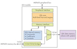
2. The low-energy accelerator is a peripheral block in the MSP430FR5994 family of RISC MCUs that’s seamlessly included in DSP operations by the compiler. (Source: TI SLASE54B)
With a 16-MHz clock, the LEA module takes less than 0.1 sec. to perform a 256-tap FIR filter operation on a block of 1,024 data points, with a power consumption of only 1.072 mA (67 µA/MHz). That’s 40X faster than competing MCUs based on the 32-bit ARM Cortex-M0+ core.
The LEA module can operate concurrently with the CPU, allowing the CPU to perform other tasks in parallel. In addition, it can operate while the CPU is in sleep mode, and trigger an interrupt when it completes the required task.
Texas Instruments also developed the MSP DSP Library with over 50 functions optimized for the MSP430 MCU. If an MSP430 configuration includes the LEA, the compiler will automatically use it to increase performance beyond that afforded by the MSP’s code-optimization feature.
Let’s take a look at two IoT applications that use the MSP430FR5994 and the LEA to perform complex DSP functions while minimizing power consumption.
Medical IoT: Holter Monitor
The healthcare field is a natural home for low-power, high-function IoT designs. Many diagnostic and monitoring procedures that formerly demanded an office visit, or even a hospital stay, are transitioning to in-home applications on mobile platforms.
For example, the electrocardiogram (ECG) is a standard test to display heart activity and help diagnose problems. But an ECG in the doctor’s office only records activity over a brief period, and may miss many abnormal rhythms and intermittent symptoms.
A Holter monitor is a battery-operated device that measures and records heart activity continuously for up to 96 hours on an AA battery. Worn by the patient, it contains electrodes that attach to the skin and helps doctors determine the cause of symptoms such as dizziness, detect pacemaker malfunctions, or assess the effectiveness of medications.
Figure 3 shows the block diagram of a Holter monitor interface based on the MSP430FR5994, an ADC, an SD card, and other peripherals.
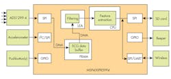
3. A Holter monitor interface design must continuously capture heart-rate data over many hours while consuming little power. (Source: TI Blog: Smart sensing with ultra-low-power MCUs – part 4: Holter monitor)
The ECG electrodes attach to the ADS1299-4, a four-channel, low-noise, 24-bit delta-sigma (ΔΣ) ADC with an integrated ECG front end. The ECG electrodes output a voltage from approximately 0.02 to 5 mV, which must be captured in the presence of much larger noise sources. These range from 50/60-Hz power-line hum to other sources in the patient’s body. As a result, the front end includes a low-noise differential-input amplifier with a high common-mode rejection ratio (CMRR). The ADS1299-4 supports a CMRR of −110 dB and operates at data rates from 250 samples/s to 16 ksamples/s.
The ADS1299-4 interfaces with the MSP430FR5994 via SPI. The MSP430FR5994 saves the SPI data from multiple ECG channels to a data buffer in the on-chip FRAM using direct memory access (DMA). This improves processing efficiency by accumulating a block of data before requiring CPU input.
At regular intervals—every second, for example—the CPU sends the data from a specific ECG channel to a buffer in the LEA RAM for filtering and additional processing. With a rate of 1 ksample/s per channel, it would take the LEA module, running at 16 MHz, about 400 ms to filter one second’s worth of data from four ECG channels. The LEA module only consumes about 0.4 mA on average during ECG data processing.
Many other effects, including poor electrode placement, can affect the quality of the results. Excessive patient movement is another culprit. The design includes an accelerometer to capture such events.
After capturing the data, the MCU430FR5994 stores the results in an SD card for offline clinical analysis. The most common features of interest include information about heart rate, variability, and the entries in a patient diary. The diary time-stamps and logs heart-rate data whenever the patient presses an event button. The design also can notify physicians wirelessly, or nearby caregivers via a buzzer, when the patient pushes the event button.
Glass-Break Detection
A glass-break detector is a sensor that generates an alarm when a pane of glass is shattered or broken. Commonly installed near glass doors or glass storefront windows, it’s a key component of building automation security systems.
When an object first strikes the glass, the contact causes the glass to emit a relatively low-frequency sound pressure wave, called the flex wave. If the glass breaks, it subsequently emits a high-frequency sound. Together, the two events make up a distinctive sound profile with a frequency content that changes over time. Different types or sizes of glass give different profiles.
A basic glass-break detector uses a microphone to detect characteristic “shattering” frequencies; it issues an alarm when the sound level exceeds a certain threshold. Since other events such as ringing bells can result in a similar frequency, the main disadvantage is a high rate of false alarms.
More sophisticated designs compare the sound to a glass-break sound profile. The method can greatly reduce false positives, but most detectors of this type compare the signal to the profile at only two or three frequencies to reduce cost and power consumption. This limitation imposes restrictions on allowable glass size, glass type, and detector placement.
Improving performance further requires a “smart” detector that can extract signature features from the glass-breaking sound to remove false positives, without imposing limitations on the type of glass or its dimensions. Figure 4 shows a conceptual system block diagram of a smart glass detector.
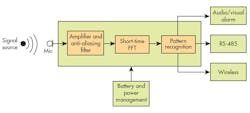
4. A smart glass-break detector must be able to perform a series of quick FFTs to extract the relevant frequency components and match them against known patterns. (Source: TI Blog: Smart sensing with ultra-low-power MCUs – part 1: glass break detectors)
The microphone shown in Fig. 4 senses the sound from the glass and outputs an analog voltage output that’s buffered, amplified, and passed through an anti-aliasing filter for sampling by the MPS430FR5994’s 12-bit on-chip ADC.
The CPU and LEA must perform two key signal-processing functions within the allotted time: short-time FFT and pattern recognition. Since the frequency spectrum of the sound changes over time, the microphone data is divided into short periods, and an FFT algorithm calculates a spectrum for each short period. This short period needs to be long enough to cover the lowest frequency of interest.
Following the FFT, the pattern-recognition algorithm examines the spectrum and its change over time to determine if a glass-breaking event is occurring. With sufficient processing power, the pattern-recognition algorithm can check the complete range of frequencies of interest instead of two to three fixed-frequency components.
For example, assume that the post-filter frequency range of the glass- breaking sound ranges from 30 Hz to 5 kHz. Then the short period must be at least 33 ms and the ADC sampling frequency must be at least 10 kHz to satisfy the Nyquist criterion. To meet this frequency range, set the period to 40 ms and the ADC sample rate to 12.8 kHz. With this period and sample rate, a 512 real-point FFT can capture a spectrum from 25 Hz to 6.4 kHz; the MCU must process this in 40 ms.
The MSP430FR5994’s LEA can easily meet this requirement. Running at 16 MHz, the LEA module can perform a 512 real-point FFT in about 1 ms while consuming zero CPU time. In comparison, a 16-MHz MPS430FR5994 performing the same operation without the LEA takes 16 ms.
Including an additional 0.5 ms of LEA time and 0.5 ms of CPU time for data movement and windowing overhead, 39.5 ms of CPU time and 38.5 ms of LEA time are available during each 40-ms interval for pattern recognition and other system functions.
How long do competing MCUs take to calculate the same 512 real-point FFT? An ARM Cortex-M0+ CPU at 24 MHz comes in at 26 ms. A more-powerful ARM Cortex-M4F CPU running at 48 MHz can match the MSP430FR5994’s time of 1 ms, but this CPU runs at three times the frequency of the MSP430FR5994 and therefore consumes considerably more power.
Fig. 4 includes an audio/visual alarm such as a buzzer or a light emitting diode (LED), plus two serial interfaces to transmit the results of the glass-break detection and allow detector diagnostics. These are:
- A wired RS-485 serial interface that’s compatible with popular building-automation standards such as Modbus and the Building Automation and Control (BAC) protocol.
- A wireless interface such as Wi-Fi, or Bluetooth.
Design Support for the MSP430FR5994
Texas Instruments offers an extensive hardware and software ecosystem for the MSP430FR599x family, including reference designs, development kits, and code examples.
Development kits include the MSP-EXP430FR5994 LaunchPad development kit and the MSP-TS430PN80B 80-pin target development board. TI also provides the free MSP430Ware software suite, available as part of the Code Composer Studio.
Conclusion
Traditionally, requiring both DSP functionality and low power consumption presented the designer with a set of opposing requirements that were difficult to reconcile. The MSP430FR5994 ultra-low-power MCU with its integrated low-energy accelerator helps solve this problem and eases the development of smart-sensing modules for IoT and other applications.
About the Author
Paul Pickering
Paul Pickering has over 35 years of engineering and marketing experience, including stints in automotive electronics, precision analog, power semiconductors, flight simulation and robotics. Originally from the North-East of England, he has lived and worked in Europe, the US, and Japan. He has a B.Sc. (Hons) in Physics & Electronics from Royal Holloway College, University of London, and has done graduate work at Tulsa University. In his spare time, he plays and teaches the guitar in the Phoenix, Ariz. area
Comment About the Article
To join the conversation, and become an exclusive member of Electronic Design, create an account today!

Leaders relevant to this article: