Mid-Range FPGAs Help Conquer Complex Communications Challenges
Download this article in PDF format.
The pressure never ends for network operators to significantly improve network capacity and coverage with limited available spectrum and capital expenditure (CAPEX) while simultaneously delivering 4K video and terabytes of other high-value content to consumers. With the rapid growth of IoT nodes, networks must securely accommodate these interfaces with minimal energy consumption while reducing operating expenditure (OPEX). Operators are also being pushed to reduce the physical and carbon footprints of their cellular infrastructure and wireline access networks.
These new market realities are making things more difficult for vendors who design communication equipment products. Today’s challenges vary in complexity, from reducing power while delivering the right transceiver rates in price-sensitive 10G wireline access and aggregations, to accommodating the special requirements of IoT gateways and C-RAN/RRH architectures as well as small-cell networks.
System architects and engineering managers must turn to suppliers that can help them create more power-efficient interfaces in smaller form factors with best-in-class security, all provided in a cost-optimized, flexible solution.
So what’s the answer? One key part of the puzzle is the need for a redefined category of mid-range field-programmable gate arrays (FPGAs)—devices that are purpose-built and specifically designed to reduce the cost, power, and size for communication applications.
New Challenges Require New Solutions
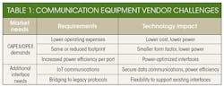
The requirements that must be satisfied by next-generation communications equipment vendors can be broken down into two categories: capital/operating demands and additional interface requirements (Table 1). Today’s mid-range FPGA architectures address these needs in multiple important ways.
First, to meet the demand for lower CAPEX/OPEX, developers are squeezing communications products into much smaller spaces. Some applications dictate a small fanless enclosure to reduce cost. Other functions may need to be crammed into small modules or add-on boards, driving the requirement for lower power consumption and smaller footprint packages while supporting interface speeds up to 12 Gb/s.
FPGAs are often a key design component and must combine adequate interface capabilities with the lowest power and smallest possible sizes. To address this, an optimized architecture with a larger capacity but a smaller physical package is required.
Many low-density FPGAs have small packages, but lack adequate interfaces (such as 12-Gb/s transceivers), while current mid-range architectures lack smaller packages and consume significant power. The crucial features that must be incorporated into smaller physical packages include 12-Gb/s transceivers, a generous amount of embedded memory, numerous 3.3-V I/Os, and interfaces to newer memory standards. The availability of FPGAs that deliver these capabilities with a power-optimized architecture for mid-range densities is a key enabler for the coming generation of small-footprint solutions.
The requirement for smaller footprints is very clear for optical modules or small-form-factor pluggable (SFP)-type modules. Many communication products have cages that can accept these interfaces and normally run at speeds from 1 to 10 Gb/s. Typically, Ethernet protocols are supported, but other interfaces are also utilized (such as CPRI, HD-SDI, HDMI, and so on).
Products that can implement functions in these modules enable additional system-level flexibility. For example, a 10-Gb/s Ethernet router may not always require synchronous network timing, such as SyncE or IEEE 1588. If an SFP cage is available, then a specifically designed SFP that supports SyncE could instead be used. This frees a system architect from having to implement the function on the router, and lowers the overall cost. Users who need the SyncE network timing can simply add the associated, specifically designed SFP module.
Although many low-end FPGAs are small enough to fit the size requirements for this application, the necessary resources are beyond the capabilities of low-end FPGAs. A typical mid-range FPGA can support 10-Gb/s Ethernet, but their power and size don’t work for these modules. Again, a mid-range FPGA optimized for cost, low power consumption, and small package sizes is needed to enable this type of design.
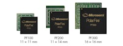
1. These compact, lower-power mid-range-density FPGAs help designers meet CAPEX and OPEX efficiency requirements.
The three CAPEX/OPEX efficiency requirements for these new types of solutions are lower power, small physical packages, and optimized mid-range density architecture. Figure 1 shows an example of FPGA devices that meet these requirements.
Revolutionary Interfaces
Power-efficient interfaces are driving changes in system architectures. Many communication-product developers are using Gigabit Ethernet for an increasing number of connections. No longer only for data payloads, these links are becoming ubiquitous for control, management, status, and more.
Traditional mid-range FPGAs require transceivers to implement SGMII interfaces, which are precious and often scarce for many designs because they’re also used for protocols like 10-Gb/s Ethernet, CPRI, JESD204B, and PCIe. Previously, designers had to use larger packages with additional transceivers, or move to FPGAs with higher logic-element (LE) counts, increasing both power consumption and cost in opposition to OPEX demands.
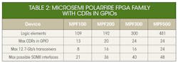
A new class of power-optimized, mid-range devices addresses this key concern. Incorporating a clock- and data-recovery (CDR) circuit into high-speed, low-voltage differential-signaling (LVDS) I/Os that can run beyond 1.25 Gb/s makes it possible to support SGMII interfaces (Table 2). Designers needn’t select larger package devices with additional transceivers, reducing cost. These GPIO CDRs also consume less power than a transceiver, thus reducing power consumption for applications using multiple GbE links, and ultimately offering a valuable strategy for reducing CAPEX/OPEX.
The second major requirement—accommodating additional interface requirements—is as important and challenging as driving down CAPEX/OPEX. Concerns here include supporting IoT communications with a focus on secure data communications and power efficiency, and bridging to legacy protocols, which requires sufficient flexibility to support existing interfaces.
Staying Secure
With network infrastructure growth now being driven by accelerated adoption of IoT applications, securing data communications has become a critical system requirement. Many hardware engineers believe security is a software problem, but nothing could be further from the truth. The data security of a system must be incorporated in the hardware, and system architects need to take responsibility for solving this issue.
Ensuring that data communications are secure requires encryption of the information being sent and decryption of the data on the receiving side. But these requirements are only a high-level answer. A specific algorithm and keys are needed as a base to provide the encrypted data.
There are many common algorithms, including AES-256, SHA, ECC, and others. To utilize these algorithms, they must be based on a key. For connection to the cloud, a dual-key public-key-infrastructure (PKI) strategy must be employed. It’s based on using both public keys and private keys. Each node on the network has a public, certified key that’s signed or approved by a trusted third party, and every node also has its own private key that only they know about.
During this type of secure communication, the sender uses a combination of its private key to encrypt the data and the receiving node’s certified public key. Only with both the public and private key can data received at the node be decrypted. Having the complete capability for securing data communications this way inside an FPGA makes it easier for architects to ensure the system’s data is protected.
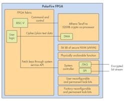
2. Microsemi’s PolarFire FPGA incorporates a data security processor, physically unclonable function (PUF), random number generator, and secure non-volatile memory.
The necessary on-chip building blocks for this capability include a cryptographic processor, physically unclonable function (PUF), key storage, and a random number generator (Fig. 2). The designer simply programs the processor to generate the key based on the on-board PUF, then selects the encryption algorithm to be used (such as AES 256), and the crypto processor performs all required functionality. The majority of the FPGA fabric is used to implement the specific design, with very few resources allocated to securing communications.
Even as developers support these emerging IoT security requirements, they also must be able to bridge to legacy protocols. FPGAs are ideally suited for this task because of their programmable fabric and I/O flexibility. Legacy interfaces as well as new protocols are supported in this new class of mid-range FPGA devices, allowing architects new levels of system-level flexibility.
The evolving demands of the communications marketplace necessitate that engineers look for new solutions. Mid-range-density FPGAs are now available to address the new challenges faced by many wireline and wireless communications vendors. No longer are designers forced to sacrifice cost and power efficiency to achieve the necessary performance. The new class of mid-range FPGAs offers lower power, smaller size, optimized interfaces, and proven data security to meet the new demands of the communications market.

About the Author

Ted Marena
Director of Business Development & Outbound Marketing
Ted Marena is the director of business development & outbound marketing at Microsemi, a wholly owned subsidiary of Microchip Technology Inc. He has over 20 years' experience in FPGAs. Previously, Marena held roles in design engineering, technical sales/support, business development, product & strategic marketing. He was awarded Innovator of the Year in February 2014, when he worked for Lattice Semiconductor.
Marena has defined, created and executed unique marketing platform solutions for vertical markets including consumer, wireless small cells, industrial, cameras, displays, and automotive applications. Marena holds a Bachelor of Science in electrical engineering Magna Cum Laude from the University of Connecticut and a MBA from Bentley College's Elkin B. McCallum Graduate School of Business.
Comment About the Article
To join the conversation, and become an exclusive member of Electronic Design, create an account today!

Leaders relevant to this article: