What’s the Difference Between All Those Emerging Memory Technologies?

Download this article in PDF format.
Nothing has stayed “new” as long as emerging memory technologies. Whether MRAM, PCM, ReRAM, or FRAM (or the many other names these technologies go by), these names have been bandied about as the “Next Big Thing” for decades, yet they never have hit the mainstream.
Let’s have a look at the leading ones, learn why they are considered necessary, and discover why they have taken as long as they have to become mainstream.
Why They’re Necessary
Chip costs are determined by two factors:
- The cost of manufacturing a silicon wafer.
- The number of chips that can be produced on that wafer.
Semiconductor manufacturers have historically used process technology shrinks to increase the number of chips that can be produced on that wafer and drive down the costs out of their chips, migrating from a 35nm process to 25nm, then 20, and so on.
As a general rule the cost to process a silicon wafer is relatively constant, so the cost of a chip tends to decline in proportion to the process technology that is used to manufacture it (Fig. 1). As the process technology shrinks (across the bottom axis of the chart), the cost of the chip should decrease in proportion (the vertical axis).
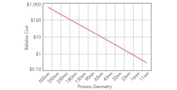
1. The relative cost of a chip is proportional to its process geometry. (Source: Objective Analysis)
Memory manufacturers believe that there is a limit to how small a flash or DRAM process can be shrunk. This is called the “scaling limit,” and is determined by the number of electrons that can be stored on a flash gate or DRAM capacitor, also called a “memory cell.” As the process technology shrinks, the memory cell gets smaller and the number of electrons the cell can store declines to approach a lower limit of what can be accurately measured. Eventually the number of electrons on the memory cell will shrink to the point that it becomes extraordinarily difficult to determine whether or not there are actually any electrons on the cell at all.
A memory cell that has been shrunk to that point can no longer shrink in proportion to the process and that means that the die size (and cost) of the flash chip will remain the same even if the production process used to make it continues to scale.
Back in 2003, Intel announced at its Intel Developer Forum that flash memory could not be scaled beyond 65nm. The company then explained its plan to move to an emerging memory technology to continue to scale past 65nm. By 2004 the company encountered a breakthrough that allowed Intel to move farther down the road, projecting that flash could scale to a 35nm process, and that Intel expected to be able to shrink even beyond that process. Then, at the end of 2007, researchers at Toshiba found a way to produce basic planar flash using an 11nm process to prove that flash memory would continue to scale for another few years.
But Toshiba also had proven a year earlier that there was a path to continue to increase the number of bits on a chip even past this point by tipping the entire structure on its side, thus creating 3D NAND. This approach further postponed the end of NAND flash, extending its life, and delaying any mass adoption of any alternative technology.
Even though the flash and DRAM businesses have enjoyed these breakthroughs, NAND and DRAM makers continue to expend significant research efforts to develop alternative technologies. From their perspective the scaling limit of today’s technologies, although frequently extended, will inevitably come upon us, forcing them to adopt some alternative technology.
Here’s how chip makers expect for this to play out. Figure 2 is a rendition of Fig. 1 meant to illustrate the relative costs of flash versus some alternative technology. The chart was actually created in 2008, nearly 10 years ago, well before 3D NAND flash was expected to extend flash technology. In the chart, wafer costs for the “New Tech” memory technology have been arbitrarily set to be 50% higher than that of standard flash. Although it’s unclear how much a new technology will actually add to the cost of a wafer in volume production, it is certain that it will increase the cost. The 50% figure fits our needs for the purpose of illustration.
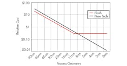
2. The end of flash scaling would open opportunities for an alternative. (Source: Objective Analysis January 2008)
This model assumed that the scaling limit for flash technology would be 10nm, which, at that time, was in keeping with Toshiba’s December 2007 announcement that was previously mentioned. (In actuality, production NAND flash stopped scaling at 15nm.)
The chart (Fig. 2) clearly shows that flash will lose its cost advantage over the new technology once flash loses its ability to scale. Although the new technology has a higher wafer cost, its ability to scale allows it to scale costs below flash’s to become the more cost-effective technology for future generations of memory. A similar chart can be drawn for DRAM.
This crossover’s timing will depend on two factors:
- The actual point at which a pure silicon flash technology loses its ability to cost-reduce; and
- The wafer processing cost difference between a pure silicon wafer and the wafer required for the new technology.
This juncture has been anticipated for over two decades, but is continually postponed. Ask any chip executive, though, and they will express certainty that a scaling limit will indeed occur, and that limit will drive the adoption of a new memory technology.
Let’s have a look at the leading alternative memory technologies.
FRAM
The Ferroelectric RAM, usually called FRAM or FeRAM, is mislabeled since it involves no iron (chemical symbol: “Fe”). Despite the technology’s name, older FRAM technologies are based on something called a Perovskite crystal. The technology gained its name from the fact that certain materials exhibit hysteresis similar to that of magnetic materials. Hysteresis is the basis for magnetic recording, and is diagrammed in Fig. 3.

3. Hysteresis (shown above) is the basis for magnetic recording. (Source: NDT Resource Center)
In a magnetic system a magnetizing force “H” is applied (horizontal axis) to push the flux density “B” (vertical axis) to be either north or south. As the force moves to the right on the chart from (0,0) the flux density of the magnet rises to some level where it saturates. When the field is removed (returning back to the center of the horizontal axis) the flux remains (marked “Retentivity”), and the bit is magnetized. The curve’s vertical axis intercept represents this remaining magnetism. Reversing this process drives the left-hand side of the curve, and causes the vertical axis to be intercepted in the opposite direction.
Ferroelectric memories behave much the same way, but the horizontal axis is replaced by the voltage across a material, and the vertical axis is used to indicate the charge.
In the past this has been accomplished through the use of certain very unique materials known as PZT and SBT. The storage mechanism consists of one atom in the middle of the PZT or SBT crystal which can be moved by a positive current to the top of the cell (the red sphere in Fig. 4) or by a negative current to the bottom to indicate a 1 or a 0. Once moved, the atom stays where it is until moved again, so the technology is nonvolatile.
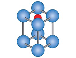
4. Here is a ferroelectric PZT molecule. (Source: Objective Analysis)
The biggest drawback that has stood in the way of the technology’s success has been that neither of the materials used, SBT or PZT, behaved very nicely in a semiconductor fabrication plant. PZT is lead zirconium titanate, and lead ions are very mobile—they wander all over the chip (and the entire fab) rather than stay where they can do their job. Lead contamination is a big concern in semiconductor fabs. This limited the technologies’ popularity.
Recently, ferroelectric-style hysteresis has been identified in hafnium oxide (HfO2), a material that is widely used in standard semiconductor processes known as Hi-k dielectrics. This is a more manageable material, and it is already used in high volume in leading wafer fabrication plants, giving it a very promising outlook for future memory technologies.
MRAM
As opposed to the FRAM, an MRAM actually does use magnetism to store bits. This makes some people worry that bits will be disturbed by external magnetic fields, but these bits are flipped by energy that is applied in very close proximity to the magnet, so the local field is extraordinarily dense compared to most externally applied fields. In other words, although you could cause bits to by applying an external magnetic field, that field would need to be extremely strong, so it would take a big effort to cause any trouble.
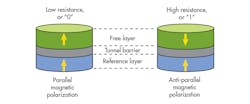
Early MRAMs, now called “Toggle MRAMs” would magnetize and demagnetize bits by passing write currents through write lines above and below the bit cell. These currents created a magnetic field around the write lines that, combined, were strong enough to magnetize the “Soft” magnetic layer represented by the green plate in Fig. 5. The blue plate, called the “hard” magnetic layer, was insensitive to this field and remained magnetized in the original direction set at the factory. Reversing the currents reversed the soft layer’s magnetic moment from north to south.

5. Above, a toggle MRAM. (Source: Freescale Semiconductor)
During manufacture a magnetic tunnel junction (MTJ) was formed between the hard and soft magnetic layers. If the two layers are both magnetized in the same direction the MTJ’s resistance is low, but if the two layers are magnetized in opposite directions then the MTJ has a high resistance.
Toggle MRAMs run into a problem as the bit cell is scaled: The current required to flip the bit doesn’t shrink as the write lines get smaller, so the current density increases to the point where the wire will melt.
The solution to this problem came from the disk-drive industry, which was already using spin torque transfer (STT, also called “spin transfer torque” in some circles) to reduce the size of the bits on HDDs. With STT the programming current actually passes through the magnet rather than through write lines adjacent to the bit. STT is the basis for more advanced MRAM cells, and a further development of STT called “perpendicular STT” promises to take MRAMs to tiny processes envisioned for future chip technologies (Fig. 6).
6. Above is a perpendicular spin transfer torque MRAM cell. (Source: Spin Transfer Technologies)
Because the materials needed to manufacture MRAM are already used in very high production volumes to make silicon-based HDD heads, their maturity is high and their interaction with silicon is very well understood. This is a strong advantage for MRAM technology.
Today MRAM is available in volume from Everspin, with other companies like Spin Transfer Technologies and Avalanche closing the gap. All of these companies are fabless. Everspin’s fab partner Globalfoundries is aggressively promoting the Everspin MRAM technology as a replacement for NOR flash in ASICs and MCUs for 14nm and tighter process geometries.
All major memory chip makers appear to have ongoing MRAM development efforts, but most are being relatively quiet about them. They’re participating in MRAM development to prepare for the inevitable end to DRAM scaling, which seems to continually be postponed.
IBM has also done some notable research on MRAMs, with the most intriguing technology being its “Racetrack Memory.” In this technology (Fig. 7), a ribbon of magnetic material is patterned onto the walls and bottom of a trench, and is treated somewhat like a magnetic tape. Read and write head structures are placed at the base of the ribbon to read and record data that runs along the length of the ribbon. When a current is passed through the ribbon the magnetized domain walls move left or right along the current path and pass over the heads.
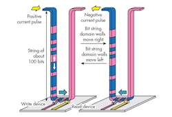
7. Here is an illustration of racetrack memory. (Source: IBM)
PCM
Perhaps the most notable attribute of Phase-Change Memory (PCM) is its legacy: Gordon Moore and Ron Neale co-authored an article in Electronics Magazine in early 1970 detailing a 256-bit PCM they had developed.
PCM works by changing the phase of a special kind of glass (Ge2Sb2Te5) within the bit cell. When a programming current flows through the cell (Fig. 8), it heats up. A higher heating current that is removed early causes the glass to solidify into an amorphous, nonconductive state. Slower heating at a lower initial temperature solidifies the glass in a conductive crystalline structure. Technically the amorphous state is still a liquid, and technically a crystal is necessarily a solid, so the two states of the cell, crystalline and amorphous, represent two of the three phases of matter: solid, liquid, and gas. This is the basis for the name “Phase Change Memory.”
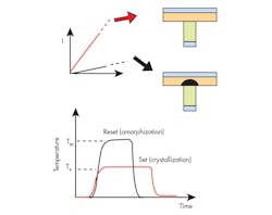
8. PCM works by changing the phase of a special kind of glass (Ge2Sb2Te5) within the bit cell. (Source: Intel Corp.)
Although Intel and Micron argued at its 2015 introduction that their new 3D XPoint Memory was not a phase change memory, reverse engineering of actual devices indicates otherwise.
One of the nicer aspects of PCM is the fact that the current runs in only one direction, making the selector much easier to design. A simple diode is all that’s needed (more on this later).
RRAM
Here’s where nomenclature gets tricky. Resistive RAM, known as RRAM or ReRAM, is an umbrella term for any memory whose bit state is defined as a higher or lower resistance. This differs from NAND and NOR flash as well as EPROM and EEPROM, all of whose states are defined by a shift in a transistor’s threshold voltage. It also differs from DRAM, whose state consists of a charge (or lack of charge) on a capacitor, or SRAM, whose state is the status of a flip-flop: Is the right-hand or the left-hand transistor turned on, since they can’t both be on at the same time?
It happens that MRAM’s mechanism involves a change in resistance, so a liberal interpretation of RRAM could include MRAM, and for similar reasons PCM could be called an RRAM.
Typically, though, the industry refers to other technologies as RRAM, mainly oxygen vacancy memory (OxRAM, below) and conductive bridging memory (CBRAM, further down).
OxRAM
The oxygen displacement memory (OxRAM) is based on a material similar to that used in PCM. This material, called chalcogenide glass, can be coupled with other materials that will remove oxygen ions when a current flows in one direction, and replace them when the current flows in the other direction. Normally this glass is an insulator, but glass with “oxygen vacancies” is conductive.
A number of different companies have research efforts in this area, including Rambus (through its acquisition of Unity Semiconductor), Western Digital (via its Contour Semiconductor acquisition), HP, 4Ds, and Weebit Nano.
One overhyped rendition of an OxRAM was HP’s “Memristor.” Although the company made out that this was a revolutionary change and was unlike any technology that had preceded it, close inspection revealed that it was yet another name for an oxygen vacancy memory.
Nano-Metal Filament
Crossbar is making serious progress in this effort with active sampling of ReRAM prototypes based on a unique nano-metal filament approach.
Crossbar’s design (Fig. 9) has been called “self-selecting” thanks to an attribute that eliminates the need for a selector device on the cell. An un-programmed cell has no naon-metal filament and does not conduct current. By passing a higher current in the right direction a conductive path is formed that almost bridges the gap, but not quite. When a small Read current is passed through the device in the same direction, the final gap is bridged and the bit becomes fully conductive.
9. Crossbar’s design has been called “self-selecting” thanks to an attribute that eliminates the need for a selector device on the cell. (Source: Crossbar Technology)
A small reverse read current (leaked from another cell) fails to bridge the gap, to prevent the “Sneak Paths” explained below. A larger reverse current removes the conductive path altogether.
CBRAM
Like the OxRAM and filament memories just described, a Conductive Bridging RAM (CBRAM) is based on a chalcogenide glass, but its set/reset mechanism differs: Rather than building a conductive path through oxygen vacancies, the CBRAM moves silver ions from the cell’s anode into the glass to create a conductive path (Fig. 10). A reverse current moves these silver ions back into the anode.
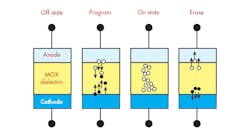
10. The CBRAM moves silver ions from the cell’s anode into the glass to create a conductive path. (Source: Adesto Technologies)
The only company actively involved in CBRAMs at this point is Adesto Technologies, whose device was initially developed at Arizona State University.
NRAM
The Nantero NRAM is a very different form of cell that uses a pad or “fabric” of carbon nanotubes (CNTs) in a silicon well to store bits (Fig. 11).
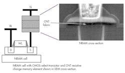
11. The Nantero NRAM uses a pad or “fabric” of carbon nanotubes (CNTs) in a silicon well to store bits. (Source: Nantero)
When a current flows through the cell in one direction these nanotubes compress into a highly-conductive state. When the current is reversed the nanotubes expand and become less conductive. Programmed bits remain in their compressed state after current is removed thanks to van der Waals forces, a phenomenon that causes things to stick together once they come into intimate contact. This is a very strong force and is a challenge to overcome in many mechanical systems, but in the case of the NRAM it is a desirable attribute.
Nantero has licensed Fujitsu to produce its NRAM technology, which is a very good sign: Fujitsu was the highest-volume producer of Ramtron’s FRAM technology in the previous two decades, having chosen this technology because of its very low write energy requirements. Fujitsu’s approval of the NRAM process is a very positive sign.
Bulk Switching
Some companies argue that there’s a statistical chance that “filamentary memories” can have bad bits, and that the likelihood that a bit will reliably program drops as the production process shrinks. The memories that do not count on filaments include PCM, MRAM, NRAM, and 4DS’ rendition of OxRAM. To our knowledge all the others use filaments to form the conductive path between either end of the bit cell.
Selector Devices
One very important part of all of these memories is the choice of selector devices. Since none of these new technologies depends on the use of transistors for sensing, they can be built as diode arrays with the memory cell above or below the diode. This automatically brings space savings to the device, since diodes are smaller than transistors.
The selector needs to have a very high ratio of on to off resistance, since a crosspoint can leak currents from unselected cells. An entire article could be dedicated to these “sneak paths” so we won’t go into that in detail here. Suffice it to say that R&D labs are placing a phenomenal focus on selectors, as is evidenced by the fact that, for the past few years the IEEE’s IEDM conference has included roughly as many selector papers as memory cell papers.
Certain companies claim to have an advantage in this realm: Crossbar’s cell is “self-selecting”, so the selector is inherently a part of the cell. PCM, including the Intel-Micron 3D XPoint Memory, is unique in that it is programmed and erased with currents flowing in the same direction. This means that the selector can be a simple diode, whereas other selectors are bidirectional devices.
The selector device is about as important as the memory cell itself, as it can make or break the memory. In the future we anticipate continuing focus on this critical technology.
Kilopass VLT
This article would be incomplete if it omitted one more technology. Kilopass has recently started to promote its VLT (Vertical Layered Thyristor) technology, shown in Fig. 12, as a replacement for SRAM and DRAM (ed. note: Kilopass was acquired by Synopsys on Jan. 10, 2018, which occurred after the writing of this article). The greatest difference between VLT and every other technology in this article is that VLT is not a nonvolatile memory. Instead, it’s a DRAM replacement that requires no refreshing and that promises to scale well beyond any limit that DRAM may face.
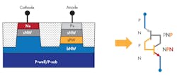
12. Kilopass has recently started to promote its VLT (Vertical Layered Thyristor) technology, as a replacement for SRAM and DRAM. (Source: Kilopass)
The bit consists of nothing more than the basic thyristor (a 4-layer device, similar to two bipolar transistors, NPN and PNP, tied together) and requires no DRAM capacitor. A selector is not required either, since the device passes current in only one direction when turned on. The bitline ties directly to the cathode and the wordline to the anode.
Not only should VLT scale well, but the company says that it also can be stacked, an option that appears today to be impossible with DRAM.
Since it’s an all-silicon technology and is based upon existing process technology it could have strong advantages over other technologies as a DRAM replacement.
Do Some Applications Prefer One Over The Other?
I am often asked which memory technology has the best prospects for success, and which applications are better matched to which technology. My short reply is that none of these technologies is particularly better suited for an application than is any other, and that cost is the one overriding factor that will determine their success.
A glowing example can be found with today’s mainstream technologies: NAND vs. NOR vs. DRAM vs. SRAM. Each of these technologies competes against the others in many applications, even though they are extremely different from one another. Code can be executed directly out of NOR but not from NAND, but NAND is substantially less costly, and NAND/DRAM combinations have successfully taken the bulk of the cell phone market from a combination of NOR flash and SRAM. Server users have found that they can often cost-reduce their systems by reducing DRAM and increasing the use of NAND-based SSDs to achieve the same performance. NOR and SRAM win out for reasons of speed or economy when the size of the memory is small enough that a cheaper NOR flash or SRAM can replace a significantly larger (and slightly more expensive) NAND or DRAM.
Decisions of which technology to use most often are based on the total cost of the system and the performance it must achieve. At the moment all of the emerging memory technologies defined above are challenged to approach the cost of entrenched alternatives – today there is a difference of a few orders of magnitude for most systems. As volume shipments increase that situation should change.
Which Will Win?
Objective Analysis expects for the memory that races down the cost curve the fastest will stand the greatest chance of winning the bulk of the market.
Intel is forcing its 3D XPoint Memory down the cost curve by manufacturing significant volumes at a loss. The company can afford to do this because it believes that 3D XPoint is required to support the company’s higher-performance CPUs. Any money that Intel loses on 3D XPoint sales will be recovered through the sale of more costly processors.
Other technologies don’t have this advantage, and must be sold at a profit to make any sense. This is a chicken-and-egg problem: To reach high volumes any emerging memory must sell at competitive prices, but costs will prohibit that until high volumes are reached.
If DRAM and NAND flash do finally hit their scaling limits, then these technologies can become cost competitive after a couple of scaling nodes have been missed, as was shown in Fig. 2, but until that time they will be relegated to those niches that can tolerate their higher costs in return for some indispensable technical advantage, and those applications are very few, and have very low unit volume requirements.

About the Author

Jim Handy
General Director, Objective Analysis
Comment About the Article
To join the conversation, and become an exclusive member of Electronic Design, create an account today!

Leaders relevant to this article: