Download this article in PDF format.
For the most part, embedded FPGA can be viewed as a “black box,” which is effectively as an RTL engine. However, sometimes it’s helpful to understand what’s going on underneath the hood to evaluate applications and competitive alternatives. This article will provide a close-up view and discuss how embedded FPGA works in general.
What is an Embedded FPGA?
An embedded FPGA is an IP block that allows a complete FPGA to be incorporated in an SoC or any kind of integrated circuit (Fig. 1). While embedded FPGA is new, the idea of what used to be chips becoming IP blocks is old. For example, RAM, SERDES, PLL, and processors are all routine IP blocks today that were once standalone chips. Now FPGA is an IP block, too.

1. An embedded FPGA IP core is similar to the core on an FPGA chip.
Conceptually, it seems as simple as using the core of an existing FPGA chip, but as you’ll see, it’s really not that simple.
An FPGA is an Array of Programmable Logic
The basic building block in every FPGA is the lookup table (LUT). Different FPGAs use different-sized LUTs, but they all use some sort of LUT. A lookup table is equivalent to a RAM with the inputs being the address select lines. Since a 4-input LUT with one output has 16 possible input states, it requires 16 configuration bits that can be programmed to implement any Boolean function. The LUT can be 5-input or 6-input or any number of inputs: 2^N configuration bits are required. A LUT can also have multiple outputs so that there are two Boolean functions of the same inputs (this doubles the number of configuration bits).
To cite a particular example, we’ll use the Flex Logix embedded FPGA platform called EFLX, since that platform has the most public information available on its website. In the second generation (Gen2) of EFLX, the LUTs are 6-input with dual outputs, and it’s configured so that it can be used as dual 5-input LUTs or a single 6-input LUT (Fig. 2).
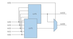
2. The 6-input LUT shown can also be used as dual 5-input LUTs.
In almost all FPGAs, LUTs are typically grouped in fours so that carry arithmetic can be added for easy implementation of N-bit counters/adders. Also, there’s an optional flip-flop on the output for pipelining. To achieve performance in an FPGA implementation of RTL, typically fewer LUT stages are between pipeline flops. Since flops are at every LUT output anyway, pipelining has no incremental cost.
Figure 3 shows the Gen2 EFLX embedded FPGA implementation of what’s called a Reconfigurable Building Block (RBB L). Xilinx calls a similar grouping a “CLB” or configurable logic block. A RBB M is similar, but the LUTs are implemented whereby they can also be used as scratch-pad memories or shift registers.
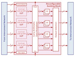
3. This Reconfigurable Building Block has four 6-input LUTs, carry logic, and eight optional flip-flops.
The I/O of an embedded FPGA is just CMOS “pins” using standard cells. The I/O is programmable so that the inputs can be flopped or go directly in, and the outputs can be flopped or go directly out (Fig. 4).
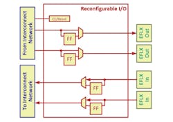
4. Reconfigurable I/O in embedded FPGA is simple, fast, and low latency.
It’s recommended to keep the timing between the hardwired logic easy to synchronize with the embedded FPGA to always flop the inputs and outputs, enabling the boundary to be fully synchronous. In some cases, this may not be desirable and asynchronous inputs/outputs are possible, but this raises challenges and increases design risk.
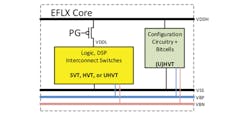
The building blocks RBB (L and M) and I/O are assembled in an array to implement a small ~100 LUT FPGA IP core (Fig. 5, lower left). The EFLX-100 IP core is a complete, small embedded FPGA with two “flavors” for logic-intensive or multiply-intensive tasks.
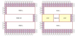
5. The EFLX-100 IP core is a complete, small embedded FPGA with two “flavors” for logic-intensive or multiply-intensive tasks.
In some applications, a need arises for extensive multiplication, which calls for another building block referred to as a MAC (multiplier-accumulator). The multiplier spec varies by vendor, but typically is a minimum of 16 × 16 bits (in EFLX, it is 22 × 22). Oftentimes, there’s a pre-adder and a post-adder as well. Figure 6 illustrates a simplified block diagram of the EFLX MAC.

6. The multiplier-accumulator (MAC) building block in an EFLX embedded FPGA has a 22-bit multiplier with a 48-bit pre-adder and a 48-bit accumulator. The MACs can pipeline from one to another without using the general programmable interconnect for higher speed.
All of the above elements are programmable, with the programming done in hardware by Configuration Memory (or Configuration Bits). The Configuration Memory is loaded at boot time with a bitstream generated by software from Verilog or VHDL RTL, which programs the logic accordingly.
Programmable Interconnect
The programmable logic has inputs and outputs that are connected with other programmable logic elements in the FPGA via a programmable interconnect. Originally, FPGAs used a mesh interconnect with “streets and avenues” of interconnect with “blocks” of programmable logic. The blocks would programmably connect inputs and outputs to the mesh interconnect, and the intersections of the mesh would involve switches to programmably steer the signals through the mesh to the destination (Fig. 7).
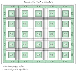
7. Most FPGA chips use a mesh-style programmable interconnect or an optimized version of one.
EFLX uses a hierarchical interconnect network (Fig. 8). This can improve density and performance. The benefit of using this hierarchical interconnect is that it reduces the area compared to the mesh, especially for larger arrays.
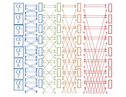
8. A hierarchical programmable interconnect network can improve density and performance.
Embedded FPGA Differs from FPGA Chips
FPGA chips are typically designed for leading-edge processes with full custom designs over a several-year period using maximum metal layers to maximize size and utilization. Embedded FPGA is an IP block that must fit with the process choices of the customer for a wide range of chips from MCUs and IoT to networking and base stations.
Embedded FPGA customers typically want the following:
- An IP block that’s compatible with their chosen process node, Vt masks, and metal stack that operates at the voltage range they prefer (most PDKs support more than one voltage range).
- Proven in silicon before they tapeout (or in the case of advanced nodes, before they start physical design).
- Available in the size they want.
- With MACs if required.
- With the type and size of embedded memory required, if any.
These requirements have numerous implications:
- The highest demand for embedded FPGA will be on the foundries and process nodes with the most design activity.
- Embedded FPGA needs to be “off the shelf” or available in approximately six months to fit in most customers’ schedules.
- Embedded FPGA suppliers need to design validation chips that allow testing of the IP at full speed with multiple RTL patterns, including stress tests, over temperature, and voltage.
- Embedded FPGA needs to use four to seven metal stacks to be compatible with all or most of the metal stacks available in a process node. TSMC 16FFC has >20 metal stacks. Up to metal 7, almost all are the same; the metal layers diverge above metal 7. As a result, an IP using 10 metal layers will only work with one or two or three of the >20 metal-stack combinations.
- To offer a wide range of sizes required, a building-block approach is ideal, since it proves out the building blocks in silicon, and then constructs arrays from the building blocks.
EFLX Embedded FPGA Arrays
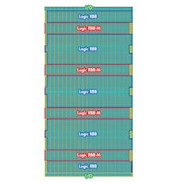
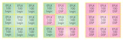
EFLX IP cores come in two sizes. The EFLX-100 IP (Fig. 9) has about 100 LUTs and the EFLX-2.5K IP has about 2500 LUTs (Fig. 10). Each comes in two flavors: one is all logic, and the other replaces some LUTs with MACs.

9. The EFLX-100 Logic IP core and the EFLX-100 DSP IP core in TSMC40ULP.
10. The EFLX-2.5K Logic IP core and DSP IP core in TSMC28HPM/HPC/HPC+.
The EFLX IP cores are complete FPGAs by themselves. Customers that want other sizes, such as 600 or 1600 LUTs, or >100K LUTs, can get them by building arrays using the N×M arrangements of the EFLX IP cores. This is possible because a “top layer” of interconnect in each IP core remains unused when the core is used as standalone, but which connects by abutment when the GDS of cores are placed side by side. Arrays can then be constructed up to 5 × 5 for EFLX-100 (Fig. 11) and up to 7 × 7 for EFLX-2.5K (Fig. 12) (the upper limits are a function of the interconnect capacity embedded in the core).
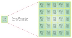
11. EFLX cores can be arrayed, in this case up to 5 × 5 for EFLX-100, to provide a quick and scalable way to deliver a wide range of sizes from silicon-proven building blocks.
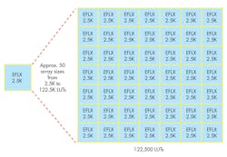
12. For EFLX-2.5K, EFLX cores can be arrayed up to 7 × 7.
The arrays can be any rectangular shape. The two “flavors” are able to be mixed to achieve the balance of LUTs and MACs that each customer wants for their application (Fig. 13).
13. The two “flavors” of EFLX IP core can be intermixed in an EFLX array to give the customer the exact right amount of logic versus MAC hardware.
Embedded FPGA Connections—Configuration, Clocking, DFT
An embedded FPGA will typically have a LOT of interconnectivity that can run at full CMOS digital speeds to enable connections to multiple wide, fast buses. The EFLX-2.5K (Fig. 14) has a total of 632 inputs and 632 outputs for a single core, and a large array can have >4000 inputs and >4000 outputs.

14. The EFLX-2.5K pins are primarily I/O with control connections for clock, power-on, configuration, and DFT.
EFLX embedded FPGA allows for two clocks per core and routes up to eight clocks across the array. Configuration is done in a row-and-column basis (configuration memory is stored in a distributed array throughout the IP core intermingled with the programmable logic and programmable interconnect circuitry). An AXI or JTAG RTL wrapper is provided for easy interface with the SoC, and design-for-testability (DFT) test vectors are supplied to achieve well over 98% stuck-at fault coverage. For the newest Gen2 EFLX cores, a new parallel test mode reduces load times for production test by 100× over the earlier generation for lower test costs and times.
Power Management in Embedded FPGA
Embedded FPGA is used in <1-MHz IoT and >1-GHz network chips. The digital architecture is similar, but the customer tradeoffs in performance, area, and power drive very different circuit implementations.
In 16 nm, networking and base stations are today’s applications, since they always demand the highest performance. In these cases, there’s no power gating because it uses up some of the IR drop budget in the chip. It’s possible to run logic at >1 GHz, but the power bussing needs to be carefully designed to handle worst-case switching conditions of >90% utilized logic with high switching rates. This is done by running Voltus simulations at worst-case PVT (process, voltage, temperature) with stress tests such as 100% utilization inverter test chains.
In 40 nm, IoT and MCUs are today’s applications, since they’re often battery-backed and require significant control over power management. For maximum power management, EFLX implements a power architecture where the configuration memory is always on. This enables the state to be maintained (until VDDH is turned off), but the dynamic logic can be power-gated to eliminate leakage power while the EFLX core isn’t operational. Some customers power-gate between clock cycles (<1 MHz IoT), and body back bias gives further control. In 40 nm, the bit cells have been designed to retain state down below 0.5 V for deep sleep and minimum power.
15. With the TSMC40ULP, multiple options exist for managing power dissipation for each of the chip's operational modes.
In TSMC40ULP (Fig. 15), customers have multiple options for managing power dissipation in each operational mode of the chip.
Connecting to the SoC Power Grid
The EFLX array, especially for high-performance advanced nodes, is designed so that power can be brought down from the SoC’s upper metal layers by going across the array to the power grid of the EFLX array. Detailed documentation is available for each EFLX IP core.
Summary
By taking an in-depth, under-the-hood look at embedded FPGA, it’s easy to evaluate applications and competitive alternatives of this powerful new technology. Now that embedded FPGA has moved from a standalone solution to being fully integrated on-chip, it has the potential to change way chips are designed and deliver substantial cost and time-to-market advantages.

About the Author
Geoff Tate
CEO and Co-Founder, Flex Logix Inc.
Geoff Tate is CEO and co-founder of Flex Logix, Inc. Earlier in his career, he was the founding CEO of Rambus where he and two PhD co-founders grew the company from four people to an IPO and a $2 billion market cap by 2005. Prior to Rambus, Tate worked for more than a decade at AMD where he was Senior VP, Microprocessors and Logic with more than 500 direct reports.
Before joining Flex Logix, Tate ran a solar company and served on several high-tech company boards. He currently is a board member of MRAM maker Everspin. Originally from Edmonton, Canada, Tate holds a Bachelor of Science in Computer Science from the University of Alberta and an MBA from Harvard University. He also completed his MSEE (coursework) at Santa Clara University.
Comment About the Article
To join the conversation, and become an exclusive member of Electronic Design, create an account today!

Leaders relevant to this article: