The Heat Is On: Protecting the LDO in Industrial Environments

Download this article in PDF format.
The Industrial Internet of Things (IoT), with its emphasis on real-time monitoring and control, has led to an explosion in the number of sensors attached to industrial machines and processes (Fig. 1). Many of the quantities being measured are analog in nature, including pressure, temperature, and flow.

1. The automated factory depends on accurate data from multiple analog sensors. (Source: TI blog: “How to ensure precision in automated processes”)
A typical data-acquisition system consists of a precision analog front end connected to the sensor, followed by an analog-to-digital converter that sends information over a wired or wireless connection to a gateway and then to the cloud.
Sponsored Resources:
Switching vs. Linear Regulators—A (Very) Short Overview
The power supply to an industrial data-acquisition system typically consists of a mix of switching and linear regulators. Each type of design has its strengths and weaknesses. At its heart, a switching design relies on a power transistor that changes the analog input voltage into a pulse-width-modulated (PWM) pulse train whose duty cycle depends on the output voltage and current. The topology chosen depends on the application. A switching regulator can convert an input voltage to a higher level (boost), a lower level (buck), or even convert a positive voltage to a negative voltage.
Switching regulators are highly efficient—up to 95% or higher—so a compact design can handle large amounts of power. The high efficiency makes a switching regulator the preferred choice for larger power-conversion tasks, such as providing an industrial rack with system dc power. To address that space, Texas Instruments has developed a wide array of switching regulators.
On the other hand, the transistor’s switching action generates noise that appears as a ripple on the output. In addition, there’s some amount of delay before the switching controller can detect and respond to sudden load changes.
In a data-acquisition system, the high level of noise is a problem when providing clean power to the sensitive analog circuitry that buffers or amplifies a low-level sensor input. That’s the domain of the linear regulator.
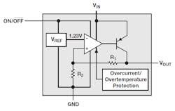
2. A linear regulator maintains a constant voltage VOUT as the load current varies. The PNP pass transistor dissipates excess power as heat. (Source: TI: “Linear power for automated industrial systems” PDF)
A linear regulator (Fig. 2) has very low output ripple and noise because it doesn’t use any switching element. Instead, its power transistor operates continuously. Any difference between the desired output voltage and the actual one is expressed as an error signal. The power-transistor control circuit uses the error signal to adjust the power transistor and move the output voltage closer to the desired value. The feedback loop is analog in nature, so the linear regulator responds instantaneously to load variations.
A linear design can only convert a higher input voltage VIN to a lower output voltage VOUT. A voltage representing the difference between the input and output (VIN − VOUT) appears across the power transistor; for a current IOUT, the power transistor therefore dissipates the wasted power as heat:
PD = (VIN − VOUT) × IOUT + (VIN × Iground)
(VIN x Iground) represents the power consumed by the control circuitry of the device. As (VIN − VOUT) increases, the linear regulator dissipates more power and the power supply becomes progressively less efficient. Therefore, the difference between VIN and VOUT should be kept as low as possible.
A linear regulator’s input voltage must be higher than the desired output voltage by a certain value—the dropout voltage VDO—to maintain regulation. If the input falls below the minimum value, the output voltage begins to decline. The value of VDO varies with input voltage, output current, and junction temperature, but a low-dropout (LDO) regulator can have a dropout voltage as low as a few tenths of a volt. Key LDO parameters include dropout voltage, output voltage, output current, input voltage range, package type, package size, control features like enable or soft-start, power-dissipation capability, and noise performance.
Texas Instruments offers over 500 LDO regulators for industrial, consumer, communications, and automotive applications.
LDO Thermal Performance and Packaging
Since the LDO dissipates excess power as heat, its thermal performance is of great interest to the designer. There are two main areas of concern: Making sure that the part doesn’t get too hot; and protecting it if the temperature exceeds a safe threshold. Let’s take a closer look at these two topics.
Why do we care about the temperature of an LDO? Although low temperatures can cause problems, in power devices we’re primarily concerned about high temperatures.
In fact, at a high-enough temperature (around 290°C for doped silicon), semiconductor action ceases—the electrical differences between the n- and p-regions disappear, and the p-n junction no longer controls the carrier flow. Long before that point, though, thermal overstress caused by excess heat melts the package, warping and cracking the integrated circuit.
There are more subtle effects, too. Many operating parameters are temperature-dependent. At high temperatures, the device may still operate, but compliance with the datasheet specifications is no longer guaranteed.
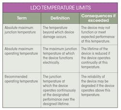
An LDO datasheet lists several high-temperature limits, as well as the likely consequences if they’re exceeded. Consult the datasheet for specifics, but the table below summarizes the results.
During operation, the LDO temperature at the junction TJ rises above ambient temperature TA due to the power PD dissipated across the pass transistor. The value of TJ is given by:
TJ = TA + (PD x RθJA)
where RθJA is the thermal resistance of the device from the junction to the ambient environment, expressed as degrees Celsius per watt. This parameter is stated in the datasheet as shown in Figure 3. It specifies the temperature rise for each watt of power consumed and is a measure of the thermal performance of the device package. You should be careful not to rely solely on RθJA to estimate the temperature of the device in the application, because the real-world value also depends on the PCB design, layout, and other factors.
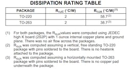
3. Many LDOs, such as the TPS759 shown here, offer a choice of packages with different RθJA values. Note that the test conditions are clearly stated. (Source: TI: “Power Good Fast-Transient Response 7.5-A Low-Dropout Voltage Regulators” PDF)
You can compare the thermal performance of two devices from different manufacturers if each one uses a standardized test, such as JEDEC’s EIA/JESD51-x standard, to measure RθJA. For more information on the thermal performance of IC packages, consult this application report.
Follow These Steps to Minimize LDO Temperature Rise
If an LDO is supplying power, its temperature is going to rise. But you can take steps to help remove the heat from the device and battle the laws of physics.
Many LDOs come in a variety of packages. Unless your design is severely space-limited, you can choose a larger, more thermally efficient package. Choosing the right package can make a big difference. The TPS732 250-mA LDO, for example, is available in three package types: an 8-pin SON (3.00 × 3.00 mm), a 6-pin SOT-223 (6.50 × 3.50 mm), and a 5-pin SOT-23 (2.90 × 1.60 mm).
The values of RθJA for these packages are 58.3, 53.1, and 205.9°C/W respectively. Why the huge variation? The SON and SOT-223 are relatively large power packages with exposed copper pads; these are soldered to the PCB ground plane and provide a thermally efficient conduit to remove heat. The SOT-23 package lacks a thermal pad; it's also the smallest in size, so it has the smallest surface area to remove heat through radiation and convection.
We can perform a quick calculation to illustrate the difference between packages in the TPS732. Let’s assume VIN = 5.5 V, VOUT = 3 V, and IOUT = 250 mA. The ground current Iground varies with temperature, VIN, and IOUT; at the maximum recommended operating temperature, 125°C, it’s about 0.72 mA.
Using the equation above gives:
PD = (5.5 – 3.0) × 0.25 + (5.5 × 0.00072) = 0.63 W
For an ambient temperature, TA, of 25°C, let’s compare TJ for the three packages:
TJ(SON) = 25°C + (58.3°C/W × 0.63 W) = 61.73°C
TJ(SOT223) = 25°C + (53.1°C/W × 0.63 W) = 58.45°C
TJ(SOT23) = 25°C + (205.9°C/W × 0.63 W) = 154.72°C
The junction temperatures for the first two packages are well within the recommended operating temperature range, but TJ(SOT23) exceeds the maximum temperature by a large margin. In fact, it’s dangerously close to the temperature (160°C) that activates the TPS732’s thermal-protection circuit.
A thermal-protection circuit is a standard feature on LDOs: When activated, it disables the output, protecting the LDO from overheating damage, and letting it cool. For the TPS732, when TJ cools to around 140°C, the thermal-protection circuit turns off, and the TPS732 resumes supplying current to the load.
If conditions don’t change, the part will heat up again and eventually reactivate the thermal protection. The LDO will continue to oscillate at some frequency that’s a function of the thermal-protection hysteresis, the power dissipation, and other variables. A calculation such as the one above is a standard part of the LDO design and would normally force a switch to a more thermally efficient package.
What other steps can the designer take to reduce the temperature rise and avoid thermal shutdown? Decreasing the thermal resistance between the LDO and the PCB is another sound strategy. If the LDO has a thermal pad, it should be soldered to the ground plane or attached to a heatsink. Much of the heat leaves the LDO via the pins, so increasing the size of the input, output, and ground planes will also decrease the thermal resistance. Most datasheets for Texas Instruments’ LDOs contain a detailed thermal analysis and layout recommendations.
Finally, you can reduce the value of PD by adding a power resistor RP in series with the LDO input. The resistor reduces the input voltage at the LDO input pin, and therefore the power that must be dissipated across the power transistor. For an input current IIN, the voltage seen at the LDO input pin is reduced by (VIN – IIN × RP).
Two cautions:
- The resistor must be able to dissipate the power PRP generated by the worst-case current (PRP = IIN(max)2 × RP)
- The voltage drop across RP when IIN(max) flows through it must leave the LDO input above the minimum needed for regulation: i.e., VIN > VOUT + VDO.
When It All Goes Wrong: Overload Protection Circuits
The design techniques discussed above are necessary, but not sufficient. As we’ve seen in the previous section, the temperature of an LDO depends on PD, which in turn depends heavily on the current IOUT supplied to the load. If the load demands more current than the LDO is designed to supply, or during an abnormal condition such as a shorted load, the LDO also contains internal circuitry to limit the current to a predefined value and prevent catastrophe.
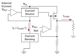
4. The LDO “brick-wall” current limit shuts off the LDO output when the load current exceeds the limit value. (Source: TI blog: “LDO basics: Current limit,” Fig. 1)
Figure 4 shows the standard LDO current-limiting circuit. It works by measuring the output current, scaling it down, and comparing the scaled current to an internal reference current IREF that represents the maximum allowed value. If the scaled output current exceeds IREF, it triggers the comparator, which shuts off the output, and the voltage drops to zero. This type of circuit is commonly referred to as a “brick-wall” current limit.
Another strategy is to limit the maximum current the LDO can supply to a fixed value ILIMIT independent of output voltage. VOUT isn’t regulated when the device is in current limit: VOUT = ILIMIT × RLOAD. If the load is shorted, the power transistor must be large enough to dissipate (VIN × ILIMIT) indefinitely—or at least until the thermal protection circuit is activated.
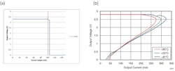
5. Two varieties of current limit: brick-wall (a) and foldback (b). (Source: TI blog: “LDO basics: Current limit,” Figs. 2,3)
Foldback current limiting is a third strategy in which the goal is to limit the total power dissipation rather than the output current. This approach keeps the output transistor within its safe power-dissipation limit by reducing the output current limit linearly while VOUT decreases and VIN remains steady. The advantage of this approach is that the foldback current is less than ILIMIT above, so the power transistor must dissipate much less power, reducing the risk of damage. Figure 5 compares the brick-wall and foldback waveforms.
Sponsored Resources:
About the Author
Paul Pickering
Paul Pickering has over 35 years of engineering and marketing experience, including stints in automotive electronics, precision analog, power semiconductors, flight simulation and robotics. Originally from the North-East of England, he has lived and worked in Europe, the US, and Japan. He has a B.Sc. (Hons) in Physics & Electronics from Royal Holloway College, University of London, and has done graduate work at Tulsa University. In his spare time, he plays and teaches the guitar in the Phoenix, Ariz. area
Comment About the Article
To join the conversation, and become an exclusive member of Electronic Design, create an account today!

Leaders relevant to this article: