For anyone looking at embedded FPGA (eFPGA), it’s important to know that the design of highly flexible, high-performance, power-efficient eFPGA isn’t enough. Customers need to be assured that the design has been thoroughly checked with advanced EDA tools for all of the critical specs—and then checked again in silicon using well-architected validation chips and automated test systems to measure all specs against actuals. With this, customers can be assured that their eFPGA will enable first-time success and make their chips more flexible and more valuable as well.
In this Q&A, Abhijit Abhyankar, VP of Silicon Engineering for Flex Logix, discusses the validation process with Electronic Design’s Bill Wong.

Abhijit Abhyankar, VP of Silicon Engineering, Flex Logix
Companies in a wide range of markets, including networking, data centers, deep learning, and more are rapidly embracing eFPGA because it significantly increases the return on investment required to bring complex chips to market. What’s driving this trend?
With readily available, high-density blocks of programmable RTL in any size and with the features a customer needs, designers now have the powerful flexibility to customize a single chip for multiple markets and/or upgrade the chip while in the system to adjust to changing standards such as networking protocols. Customers can also easily update their chips with the latest deep-learning algorithms and/or implement their own versions of protocols in data centers. In the past, the only way to accomplish these updates was through expensive and time-consuming new mask versions of the same chip.
How can chip designers make sure the eFPGA will work in their chips?
Today, a handful of suppliers offer eFPGA platforms, including Flex Logix, Achronix, Menta, and more. With so many options, it’s important that chip designers pick the best solution for their markets and applications, and that this solution works the way it should. This can only be done if the eFPGA is checked with advanced EDA tools for all critical specs, and then checked again in silicon using well-architected validation chips and automated test systems to measure all specs against actuals.
When designing an eFPGA IP core, how can engineers ensure it will meet its performance targets?
A good embedded IP core is designed in roughly six months starting from the process node’s PDK and the foundry’s standard cell library. Everything in the embedded FPGA is digital and meets logic design rules.
It’s important to have a suite of “stress test” RTL patterns to check that the netlist functions as expected. The bitstream of each of the patterns should be executed cycle-by-cycle to ensure expected and actual outputs match for each of the test patterns.
One way to ensure eFPGA meets its performance targets is to simulate the operation of the IP core using stress test bitstreams, such as inverter-chains (maximum switching activity and very high utilization). This verifies that that it achieves the performance specs within the IR-drop budget across process/voltage/temperature. Before this, chip designers must also ensure there’s a robust power grid in the IP core and that their eFPGA supplier has provided integration guidelines for connecting its IP with the power grid of the whole chip.
Since the eFGPA is integrated by the SoC/ASIC designer inside their SoC/ASIC and is powered by the SoC/ASIC VDD, the eFPGA supplier must also ensure that its eFPGA IR/EM is as good or better than the required specification of the SoC/ASIC. IR/EM is one of the crucial metrics for long-term reliability of the device.
For example, shown is a “heat-map” output of a IR simulation of Flex Logix’s smallest IP core, the EFLX-100 (Fig. 1). The simulation is run using a commercial EDA tool called Voltus. In this example, the worse-case IR drop (red portions) is 45 mV, which corresponds to <4% drop inside the eFPGA; the blue color represents close to 0% IR drop. Similar heat maps are created for power EM to ensure the eFPGA meets the requirements. Voltus is also used to simulate static, dynamic, and switching currents across any PVT corners for which standard foundry LIB files are available. Post silicon, the simulation results are used to correlate measured eFPGA silicon results.
1. The IR simulation “heat map” of Flex Logix’s smallest IP core, the EFLX-100, shows how they operate with in the IR drop spec even for high utilization and maximum rated performance.
In addition to simulating for IR/EM, it’s also important for the eFPGA supplier to closely manage timing based on worst-case/best corners specified by the foundry standard cell libraries. IP cores are constrained by the standard cell library and can only close timing for corners that the standard cells have simulations for. Timing closure is achieved using static timing analysis with industry standard CCN (noise), CCSP (power) and OCV (on-chip variation) models. OCV is especially becoming a very important requirement with sub-20-nm process nodes.
Do you have to worry about manufacturing defects during this stage?
Yes. One thing that’s very important to customers is test coverage because this helps screen manufacturing defects. High coverage and test time are especially challenging for eFPGA compared to a synthesized digital design. The main difference is that the eFPGA is a blank programmable/reconfigurable array that has to be configured before running ATPG vectors.
As an example, Flex Logix implemented logic in its eFPGA IP core to enable >98.5% coverage and at the same time reduce the number of vectors needed to achieve this coverage. This results in shorter test times and a reduction in test costs. Flex Logix also developed a flow to allow eFPGA to be tested using standard ATPG tools like Mentor Graphics’ Tessent. The ASIC/SoC designer can integrate eFPGA into their ASIC/SoC and use standard ATPG flow. The company also provides ATPG test vectors to its customers for production testing.
It’s obviously important to design a validation chip when implementing eFPGA. What’s the best way to do this and what are the most important criteria to consider?
Customers always want to see IP blocks proven in silicon, even when they’re fully digital. When designing a validation chip, the following objectives should be met:
- Enable testing of the eFPGA IP at and above maximum rated performance specs.
- Enable testing at precisely constructed chip temperatures and voltages.
- Validate that the IP core is scalable to maximum array sizes.
- Keep IP licensing costs down through economical implementation.
- Enable fast design and fast testing.
In the case of Flex Logix’s eFPGA, its IP is designed to be arrayable. A single IP block is a complete eFPGA including I/O, and it contains a top level of networking circuitry. When unused in a 1×1 configuration, this enables IP cores when abutted to extend the top-level interconnect across an array of IP cores up to 5x5 (for the EFLX-100) and up to 7×7 (for the EFLX-2.5K).
Even the EFLX 40-nm IP can run at speeds above the frequency of GPIO. Clearly, trying to validate the IP by testing the chip with very-high-speed I/Os would lead to a complicated and expensive solution that might not be measuring the performance of the IP block or the analog-intensive I/Os and packaging/PCB. Instead, validation chips should only use GPIO for start and stop tests.
All of the critical at-speed testing can be conducted inside the validation chip to emulate how the embedded IP will be used inside an ASIC/SoC. If SRAM is put on chip in significant amounts, it can run RTL patterns with a significant bank of inputs and put outputs into a separate SRAM for verification that the outputs generated match expected. Essentially this is a tester on a chip.
To operate at required speeds (e.g., >1GHz for 16 nm), it’s recommended that the eFPGA runs commercially available PLLs from mainstream suppliers. The PLL enables it to take a GPIO signal and step it up to the desired frequency.
To determine with precision the on-die temperature and voltage, we recommend using commercially available PVT monitors from mainstream suppliers that tell the exact junction temperature and exact junction voltage.
Figure 2 illustrates an example of our 40-nm validation chip. In this image, five different arrays from 2×2 to 4×4 are implemented with multiple SRAMs, a PLL, and PVT monitors. Multiple arrays are implemented because in 40 nm, it can support five different combinations of VT masks. This is important because it ensures the eFPGA is compatible with the process choices customers make.
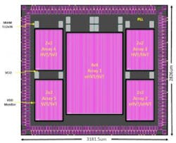
2. A 40-nm validation chip from Flex Logix has five different arrays, to test the various supported VT mask combinations, from 2×2 to 4×4. The validation chip also has multiple SRAMs, PVT monitors, and a PLL.
What is the best way to test an eFPGA validation chip?
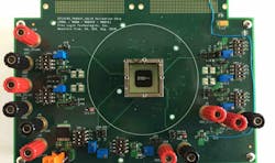
Validation chips are packaged and then mounted on a test board. Figure 3 represents an example of the test board for a 40nm validation chip.
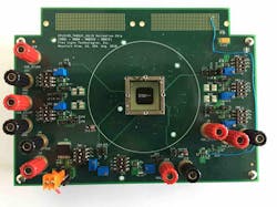
3. A validation chip is packaged and then mounted on a test board that can be coupled with a Kintex FPGA board for testing.
The test board is connected to a unit that “tests” the IP. The example in Fig. 3 uses a Kintex FPGA board. While this has worked well to date, a more preferable solution in the future is to move to a USB/PC test setup because customers are primarily chip designers and not FPGA designers.
Validation consists of testing multiple chips using multiple stress-test patterns (high-switching activity, high utilization, and intensive utilization of the different types of programmable logic blocks) across temperature and voltage to determine “shmoo” plots of performance. This is then compared to the expected results predicted for the RTL by the compiler.
Embedded IP blocks should be designed to work at multiple nominal voltages; therefore, several voltage ranges need to be checked as well. To conduct temperature testing at −40, 0, 25, and 125°C, Flex Logix has a thermal forcing system designed to mate with the test board to generate the exact temperature required. The on-chip temperature sensors give feedback so that the on-die temperature can be controlled precisely. Such a setup is shown in Figure 4.
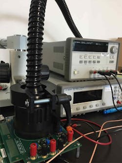
4. A thermal-forcing system mates with the test board to generate the exact temperature required.
The large number of tests and measurements can be very time-consuming if done manually, so it’s important to automate the process. This enables all tests to be done with one push of the button for a single chip across temperature and voltage, with a program controlling test setup and temperature generator. This automated validation software enables collection and testing of the eFPGA and provides performance of real user as well as synthetic benchmarks. Metrics such as speed, leakage, and dynamic currents are also measured, and these are compared with expected pre-silicon simulation metrics.
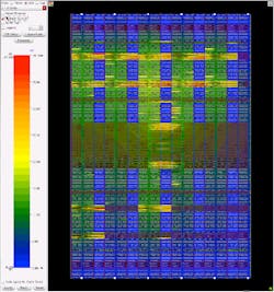
Figure 5 shows a sample of silicon validation results for EFLX-100 eFPGA IP in 40 nm. This particular RTL utilizes over 90% of the LUTs with very high switching activity (a stress test). The automated validation environment helped gather 240 data points where each “green” dot represents pass and “red” dots represent fail.
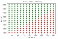
5. Example validation results for the 40-nm EFLX-100 shows a shmoo across hundreds of data points; green dots = pass, red = fail.
Automation allows for rapid margining and validation of the eFPGA. Silicon validation reports have shown 10+ stress tests and RTL representative of typical applications with measurements and shmoo plots taken at three temperatures (−40 Tj, Room, +125 Tj) at VDDMIN. This shows the predicted timing versus the measured result
Thanks Abhijit. This has been a great discussion on how to properly validate eFPGA. Anything you would like to add in closing?
For anyone looking at eFPGA, it’s important to know that the design of highly flexible, high-performance, power-efficient eFPGA isn’t enough. Customers need to be assured that the design has been thoroughly checked with advanced EDA tools for all critical specs, and then checked again in silicon using well-architected validation chips and automated test systems to measure all specs against actuals. With this, customers can be assured that their eFPGA will enable first-time success and make their chips more flexible and more valuable as well.
Abhijit Abhyankar, originally from Pune, India, holds a BSEE from the University of Utah, MSEE from Stanford, and an MBA from San Jose State. Abhijit has more than 20 years of experience in silicon and system design at LTX and then Rambus, where he was Senior Engineering Director and Technical Director. He has managed over 100 people in high-speed digital logic, mixed signal, system, verification and software teams. His projects have resulted in millions of chips and systems sold by companies such as Intel, Sony, IBM, Toshiba and others.

About the Author

William G. Wong
Senior Content Director - Electronic Design and Microwaves & RF
I am Editor of Electronic Design focusing on embedded, software, and systems. As Senior Content Director, I also manage Microwaves & RF and I work with a great team of editors to provide engineers, programmers, developers and technical managers with interesting and useful articles and videos on a regular basis. Check out our free newsletters to see the latest content.
You can send press releases for new products for possible coverage on the website. I am also interested in receiving contributed articles for publishing on our website. Use our template and send to me along with a signed release form.
Check out my blog, AltEmbedded on Electronic Design, as well as his latest articles on this site that are listed below.
You can visit my social media via these links:
- AltEmbedded on Electronic Design
- Bill Wong on Facebook
- @AltEmbedded on Twitter
- Bill Wong on LinkedIn
I earned a Bachelor of Electrical Engineering at the Georgia Institute of Technology and a Masters in Computer Science from Rutgers University. I still do a bit of programming using everything from C and C++ to Rust and Ada/SPARK. I do a bit of PHP programming for Drupal websites. I have posted a few Drupal modules.
I still get a hand on software and electronic hardware. Some of this can be found on our Kit Close-Up video series. You can also see me on many of our TechXchange Talk videos. I am interested in a range of projects from robotics to artificial intelligence.
Comment About the Article
To join the conversation, and become an exclusive member of Electronic Design, create an account today!

Leaders relevant to this article: