
Download the PDF of this article.
If you haven’t heard about the artificial intelligence (AI) machine-learning (ML) craze that uses deep neural networks (DNN) and deep learning (DL) to tackle everything from voice recognition to making self-driving cars a reality, then you probably haven’t heard about Google’s new Tensor Processing Unit (TPU), Intel’s Lake Crest, or Knupath’s Hermosa. These are just a few of the vendors looking to deliver platforms targeting neural networks.
Google TPU
The TPU contains a large 8-bit matrix multiply unit (Fig. 1). It essentially optimizes the number-crunching required by DNN; large floating-point number-crunchers need not apply.
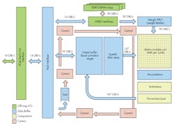
1. Google’s TPU has a large 8-bit matrix multiply unit to help it crunch numbers for deep neural networks.
The TPU is actually a coprocessor managed by a conventional host CPU via the TPU’s PCI Express interface. The TPU chip runs at only 700 MHz, but can best CPU and GPU systems when it comes to DNN acceleration. Though not specifically a DNN processor, it handles the heavy lifting while consuming only 40 W of power. It has 28 Mbytes of on-chip RAM along with 4 Mbytes in the form of 32-bit accumulators used to compile the 16-bit results from the matrix multiply unit. The chip uses a 28-nm process and the die size is about 600 mm2. The paper “In-Datacenter Performance Analysis of a Tensor Processing Unit” provides more details.
The TPU board (Fig. 2) can perform 92 TeraOps/s (TOPS). It is 15 to 30 times faster than CPUs and GPUs tasked with the same work, with a 30- to 80-fold improvement in TOPS/W. The software used for comparison of systems was the TensorFlow framework.
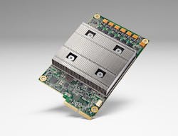
2. Google’s TPU module is designed to fill arrays of slots in its cloud data centers.
One thing to keep in mind is that TPU comparisons are done with respect to its limitations. Most CPUs are 64-bit platforms and GPUs can have wider word widths. They also tend to be optimized for larger data items, although most systems have support for smaller word sizes (including 8-bit vector operations). Likewise, different neural network applications benefit from different configurations, but the smaller 8-bit integers have found wide application in many DNN applications.
The TPU is has five primary instructions:
- Read_Host
- Read_Weights
- MatrixMultiply/Convolve
- Activate
- Write_Host
Weights are values within a neural network and are used by the matrix multiply unit. The activate function performs a nonlinear operation for an artificial neuron.
Google’s TPU is expected to reduce the need for larger data centers that would otherwise need many more CPUs and GPUs to handle the AI applications addressing everything from voice recognition and analysis, to image and video processing, to providing services from search, to those little Google Home systems.
Intel Lake Crest
Lake Crest (Fig. 3) is the codename for an Intel platform designed to complement the many-core Xeon Phi. The Xeon Phi has been tasked with many AI chores, but it can be challenged by applications that Google’s TPU or Intel’s Lake Crest will readily handle more efficiently. Lake Crest technology was originally developed by Nervana, which is not part of Intel.
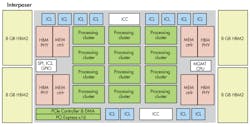
3. Intel’s Lake Crest uses processing clusters optimized for AI applications.
The new chip will employ a range of advanced features from MCM (Multi Chip Module) design to the “Flexpoint” architecture with a dozen specialized, multicore processing nodes like the TPU’s matrix multiply unit. The chips will have 32 Gbytes of High Bandwidth Memory 2 (HBM2) with an aggregate bandwidth of 8 Tbytes/s attached via an interposer. HBM2 has become common in high-performance SoCs and GPUs. Lake Crest does not have any caches. Software will be used to optimize memory management.
Lake Crest is expected in the 2017 timeframe.
Knupath Hermosa
Knupath’s Hermosa (Fig. 4) has 64 DMA engines and 256 DSP cores organized in eight clusters of eight cores connected by its Lambda Fabric. The Lambda Fabric is also designed to link thousands of Hermosa processors in a low latency and high throughput mesh.
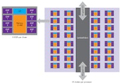
4. Knupath’s Hermosa many core processor has 256 DSP cores organized in eight clusters of eight cores connected by its Lambda Fabric.
The Hermosa has an integrated L1 router with 32 ports and a 1 Tbit/s bandwidth. Links to the outside world include 16 10 Gbit/s bidirectional ports. The chip has 72 Mbytes of data RAM organized in 32 banks and 2 Mbytes of program RAM.
Although Hermosa targets AI applications, it may be more akin to the many core Xeon Phi than the more specialized Lake Crest or TPU platforms. Hermosa only uses 34 W to deliver 384 GFLOPS of computing power, making it very interesting for a wide range of applications—not just AI ones.
GPGPUs Continue to Reign (for Now)
NVidia and AMD have a vested interest in their GPU platforms, which have been the backbone for most high-end neural network work. This could change as specialized AI chips become available. The question is how tailored these chips will be to a particular application, how available they will be, and how well they can be applied to different applications.
Right now GPU platforms like NVidia’s Jetson TX2 are being used in everything from drones to medical devices. It is actually possible to be used in an AI accelerator in Intel’s tiny Curie module, as well. One size does not fit all, but AI will only continue grow in importance for computer applications.

About the Author

William G. Wong
Senior Content Director - Electronic Design and Microwaves & RF
I am Editor of Electronic Design focusing on embedded, software, and systems. As Senior Content Director, I also manage Microwaves & RF and I work with a great team of editors to provide engineers, programmers, developers and technical managers with interesting and useful articles and videos on a regular basis. Check out our free newsletters to see the latest content.
You can send press releases for new products for possible coverage on the website. I am also interested in receiving contributed articles for publishing on our website. Use our template and send to me along with a signed release form.
Check out my blog, AltEmbedded on Electronic Design, as well as his latest articles on this site that are listed below.
You can visit my social media via these links:
- AltEmbedded on Electronic Design
- Bill Wong on Facebook
- @AltEmbedded on Twitter
- Bill Wong on LinkedIn
I earned a Bachelor of Electrical Engineering at the Georgia Institute of Technology and a Masters in Computer Science from Rutgers University. I still do a bit of programming using everything from C and C++ to Rust and Ada/SPARK. I do a bit of PHP programming for Drupal websites. I have posted a few Drupal modules.
I still get a hand on software and electronic hardware. Some of this can be found on our Kit Close-Up video series. You can also see me on many of our TechXchange Talk videos. I am interested in a range of projects from robotics to artificial intelligence.
Comment About the Article
To join the conversation, and become an exclusive member of Electronic Design, create an account today!

Leaders relevant to this article: