Today’s electronic packages have high clock speeds (multi-gigahertz range), fine pin densities (below 0.4-mm pitch), and high pin counts (over 2000). When assembled onto a printed-circuit board (PCB), these packages perform certain functions at certain speed. Attaching these packages through an IC socket is one way to test the functionality of IC packages without damaging it.
This file type includes high resolution graphics and schematics when applicable.
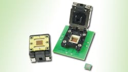
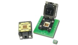
Connecting these high-speed and high-density IC packages requires an innovative solution to overcome the challenges of designing a shorter signal path (less resistance), good electrical insulation (prevents signal loss), and proper thermal management. Socket design is dictated not only by the aforementioned functions, but also by the other parameters such as durability, power consumption, assembly methods, and the operating environment. An IC socket using elastomer interconnect provides a solution that is fast, dense, and durable (Fig. 1).
Socket Function
A socket can be defined as an electromechanical device that provides a removable interface between the IC package and system circuit board with minimal effect on signal integrity. A removable interface—the primary reason for using a socket—is required for a variety of reasons, including ease of assembly, reworking, upgrading, and cost savings. The cost advantage comes from not having to attach the IC permanently to PCB. The socket is semi-permanently (solderless) attached to the PCB, while the IC device can be inserted into, or removed from, the socket without disturbing the connections to the PCB.
A socket helps to test, evaluate and inspect the complete system. It also allows for in-the-field maintenance, testing, replacement, or upgrades. This has become ever-more critical as technology evolves. The PCB surface to which the socket is attached needs to meet certain constraints (pad size, location, plating finish, etc.) to function properly. In this article, we examine the impact of different plating finishes on the PCB pads, and how it affects testing IC devices using an elastomer interconnect socket.
Elastomer
Elastomer is a contact technology that interfaces the solder ball from the device to a contact pad in the PCB. The elastomer consists of a fine-pitch matrix of gold-plated wires that are embedded at a 63° or 90° angle in a soft insulating sheet of silicone rubber. The gold-plated brass filaments protrude several microns from the top and bottom surfaces of the silicone sheet.
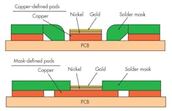
Solder balls from the IC package come in contact with the top end of the elastomer wire. The bottom end of the elastomer wire contacts with the circuit board pad and thereby makes an electrical path for the signal. The number of wire filaments making contact depends on the solder ball and circuit-board pad diameters. Typically, a PCB’s socket footprint area is covered by a solder mask in a non-contact area. Contact pads are either manufactured with a defined solder mask or defined copper. Figure 2 shows cross-sectional view of the PCB with a copper-defined pad and mask-defined pad.
When looking at the figure, it’s evident that copper-defined pads are superior to mask-defined pads, because they allow a larger contact area specifically for the elastomer contact. This phenomenon becomes more critical when the device pitch shrinks to 0.4 mm due to the 0.25-mm contact-pad size.
Plating Test
In this experiment, copper-defined pads were fixed as one of the parameters. Four plating options—lead-free, ENIG (electroless nickel immersion gold), ENEPIG (electroless nickel electroless palladium immersion gold) plating, and hard nickel gold—were considered as variables in the experiment. We also fixed the solder-mask thickness as per IPC–SM-840D, which is 0.001 in. (0.025 mm) minimum.
Lead-free plating is accomplished by dipping the PCB in a lead-free solder bath and blowing off excess solder using a hot-air manifold. Final plating thickness is typically 0.001 to 0.002 in. With a lead-free plating finish, PCB pads often rise above solder-mask height.
With ENIG plating, the PCB contact pad will be always fall below the solder mask. According to IPC 4552, typical nickel plating is 0.0001 to 0.0002 in., and gold plating is 2 to 9 µin. Ni+Au will be 0.000102 to 0.000209 in.
For ENEPIG, typical nickel plating is 0.0001 to 0.0002 in., palladium plating measures 10 to 30 µin., and gold plating is 1 to 2 µin. Ni+Pd+Au will measure 0.000111 to 0.000232 in. As with ENIG, the PCB contact pad will be always below the solder mask when using ENEPIG.
Hard nickel gold plating is and electrolytic process. Typical hard nickel plating measures 0.0001 to 0.0003 in. and hard gold plating is 10 to 30 µin. Hard Ni+Au will be 0.00011 to 0.00033 in. With hard nickel gold plating, once again the PCB contact pad will be always below the solder mask.
Another variable used in the experiment was device pitch. Since the contact pads are proportional to device pitch, contact-pad sizes increase or decrease corresponding to device pitch. Three different devices (0.4-, 0.5- and 1-mm pitch) are typically used for this experimentation.
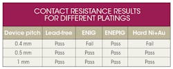
Sockets with elastomer contact were assembled onto PCBs with different plating. Devices were placed inside the socket and actuated. Subsequently, contact resistance was measured—if the contact resistance was below 50 mâ¦, then it is considered as a “pass.” After that, the process was repeated for 50 cycles. If in any one instance the contact resistance rose above 50 mâ¦, then it is considered as a “fail” (see the table).
The table reveals that the PCB contact-pad plating variation did not affect devices with a pitch of 0.5 mm or larger. However, PCBs with ENIG and hard Ni+Au plating were not connecting well for the 0.4-mm pitch devices. One reason is because the 0.4-mm pitch has a contact-pad size of 0.25 mm round. Another is the fact that these two plating options were well below solder mask height. Furthermore, the elastomer’s stiffness makes it very difficult to deflect and contact such a small contact-pad area, which is recessed below solder mask.
This file type includes high resolution graphics and schematics when applicable.
Conclusion
A primary concern to anyone utilizing high-density devices is that the socket must provide a high-performance, low and stable value of contact resistance while meeting mating requirements—specifically mating force and the number of mating cycles it must withstand without degradation. PCB plating finish plays a major role in meeting the socket’s functional requirements. Devices used in high-speed, high-density, high-pin-count applications need special consideration in terms of PCB finishes and socket contact selection. The test results given here illustrate the constraints of PCB plating finishes with respect to an elastomer contact. When a specific contact finish is required by the application, then PCB contact-pad plating thickness needs to increase for smaller pitch devices.
Ila Pal, COO for Ironwood Electronics, holds an MSME from Iowa State University and an MBA from St. Thomas University. He has six patents, published many articles, and presented a number of papers. He can be reached at [email protected].
About the Author
Ila Pal
COO
Ila Pal, COO for Ironwood Electronics, holds an MSME from Iowa State University and an MBA from St. Thomas University. He has six patents, published many articles, and presented a number of papers.
Voice Your Opinion!
To join the conversation, and become an exclusive member of Electronic Design, create an account today!

Leaders relevant to this article:


