This file type includes high resolution graphics and schematics when applicable.
Memory plays a continually more important role in digital and mixed-signal circuits, but a key for future designs is minimizing the amount of chip area occupied by high-speed memory circuitry. According to an earlier forecast by the International Technology Roadmap of Semiconductors (ITRS), memory will occupy at least 90% of a digital chip’s area by 2013.1 The performance of system-on-chip (SoC) devices will increasingly rely on the capabilities of static random-access-memory (SRAM) circuitry, encouraging the development of higher-performance SRAM.
High-performance process technologies, such as 65-nm silicon CMOS, offers the means for producing higher-performance SRAM while also maintaining compact size. Scaling technology, however, has deteriorated the stability of conventional six-transistor (6T) SRAM cells.
This occurs for several reasons, such as process variations that happen during manufacturing, which lead to SRAM transistor parameter variations.2,3 In addition, threshold mismatches can occur due to intrinsic device fluctuations, significantly reducing an SRAM cell’s static noise margin (SNM). As a result, external noise can disrupt the SRAM voltage during a read operation.4,5 Also, growing consumption of memory by leakage energy shrinks the effective amount of memory for an SRAM device. In modern microprocessors, leakage current consumes more than 40% of total active-mode energy.6
For these reasons, the need for a stable, low-power, high-speed SRAM design for microprocessors and SoCs became evidently clear. The design is a 16-kb, triple-port (one write port and two read ports, or 1W2R), 10-transistor (10T) SRAM cell. Here, the SNM is much higher than in a conventional 8T SRAM cell, and supply-voltage variations exert little effect on read SNM.
One large advantage that 8T SRAM cells offer over 6T SRAM cells is that they can be readily scaled with technology, although 8T cells will be limited by supply voltage and SNM. Figure 1 compares memory-cell areas for 6T and 18T SRAM at supply voltages of +1.0 and +0.8 V dc, considering a six-sigma threshold variation. The minimum width and length of the SRAM cell areas are assumed to scale by a factor of 0.7 per cell generation. As the plots show, the 6T and 8T curves meet at a supply voltage of +1.0 V dc for a 45-nm CMOS technology node and at +0.8 V dc for a 65-nm node. For a +1.0-V dc supply, the area for standard 8T SRAM becomes smaller than standard 6T SRAM for a 32-nm node. If the voltage supply is reduced to +0.8 V dc, the area of the standard 6T SRAM cannot be shrunk further due to the large width that’s required for the pull-down transistors in the 6T memory structure.
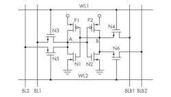
Figure 2 shows a conventional double-read-port eight-transistor (8T) SRAM cell with a structure similar to that of a 6T SRAM cell, although it contains two sets of access paths. Each access path can accomplish write and read functions independently. The stability of the 8T SRAM cell depends on the strengths of the cell transistors, referred to as the γ ratio for the write function and the β ratio for the read function. Parameter γ is the ratio of the pull-up transistors (P1 and P2) and the access transistors (N3 and N4), while parameter β is the ratio of the access transistors and the pull-down transistors (N1 and N2).
Increasing SNM typically involves large-dimensioned pull-down transistors. But such an approach to enhancing SNM usually results in limited SRAM cell area, high leakage, and limited supply voltage. Also, semiconductor process variations and threshold fluctuations can lead to uneven performance during read operations for 8T SRAM cells.
Advantages of 10T SRAM
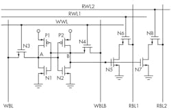
As an alternative, a triple-port 10T SRAM cell structure with single-ended readout (Fig. 3) offers a similar approach to that of 8T SRAM, but with some performance advantages. It has two read ports and achieves a high static noise margin with the separate ports.
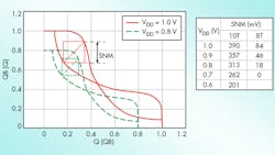
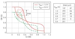
Figure 4 provides simulation comparisons of 8T and 10T SRAM designs based on 65-nm technology. The 8T SRAM cell has 84-mV SNM, while the 10T SRAM cell possesses 390-mV SNM at +1.0 VDD. When VDD drops to +0.8 V dc, the SNM of the 8T SRAM cell reduces to 18 mV while the SNM of the 10T SRAM cell is 313 mV. Separate read ports make it possible to shrink the dimensions of the 10T SRAM cell transistor, as well as reduce cell voltage leakage. The stacked NMOS transistors used in the read port can also help diminish cell leakage.
The decoder, which decodes an address into word lines, is one of the most significant peripheral circuits for an SRAM device. For the memory in this report, 9-bit addresses are decoded into 512 word lines. Typically, a column-select signal has 512 write word lines and 1024 read word lines (with the two read ports) in an operation involving the 10T SRAM cells. Of course, so many read word lines are difficult to route. To reduce the amount of lines, the column-select is set for two (for the read port), except when applied to the write port. As a result, the total word lines reduce by 1024, with write and read word lines each occupying one-half of the operation.
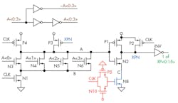
A dynamic decoder is used in the design of the 10T SRAM cells, compared to a static decoder for the 8T SRAM cells. As Figure 5 shows, a first-level predecoder in the 10T SRAM employs NOR-type gates. In the 10T SRAM cells, the switch-on transfer gates postpones opening the domino circuit until the finish of the evaluation stage for the dynamic gates, ensuring that the XPN node voltage doesn’t reach the inverter threshold and cause a wrong word-line event, helping to improve decoder reliability and efficiency.
Meanwhile, the second-level decoder employs NAND-type dynamic gates (Fig. 6). For the write port, the predecoder divides a 9-b address into 4-to-16 decoder and 5-to-32 decoder paths. Furthermore, the output of the 4-to-16 decoder is regarded as the logic input of the second-level decoder, while the output of the 5-to-32 decoder is taken as the clock input of the second-level decoder. For a read port, the most significant bit (MSB) of a 9-b address serves as the column-select signal. The other bits are separated into two 4-to-16 decoders, with one working as the logic input and the other serving as the clock input.
In conventional 8T SRAMs, the speed of SRAM access can be increased by using sense amplifiers to detect and amplify bit-line signals and eventually transform them in a read operation. During a write operation, write data are transferred to desired cells by driving data on bit-line pairs by grounding either the main bit-line or complementary bit-line. In contrast, the 10T SRAM cells export full-swing voltages by grounding the single-ended read bit-line and writing data like an 8T SRAM cell by driving data on the write bit-line pairs.
In addition, with separate read/write ports, a read/write multiplexer is not needed, which generally simplifies local evaluation circuitry and makes it possible to design a completely independent read/write path. In this way, the read scheme of the 10T SRAM cells is distinct from that of the 8T SRAM cells.
Read Paths
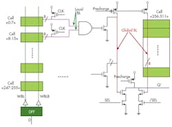
The 10T SRAM cell design employs short local read bit lines (LRBLs) and extended global read bit lines (GRBLs) for the read operation, but not a bit-line hierarchy for the write operation. Figure 7 shows the read path for transferring stored data from the cell to the memory outputs when using hierarchical bit lines. A short (8-bit) LRBL forms a high-speed full-swing local read path, while a long (256-bit) GRBL is devoted to a global read path.
The read path features two-level-selection operation. One level is 8:1 mux during LRBL operation, and the other level is 2:1 mux during GRBL operation. The major advantage of this two-level architecture is that the path of output can remove sense amplifiers and full-swing voltage preserves signal integrity, as well as speeds up read access. Because it employs a dynamic circuit on read path, the 10T SRAM consumes a little higher dynamic power versus the 8T SRAM for a read operation, and requires limited-switch-dynamic-logic (LSDL) circuits to transform a dynamic signal into a static output (Fig. 8).
The write path for the 10T SRAM cell is much simpler than for the read path. Because the write operation does not use a bit-line hierarchy, the input data is driven to the write bit-line pairs directly after being latched by the data flip-flop (DFF), as shown in Figure 7.
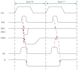
Figure 9 illustrates the simulated timing diagram of this memory in a read operation. The read bit-lines start precharged to some reference voltage that’s usually close to the positive supply. When the read word-line turns high, the access transistor connected to the cell node storing a “0” bit starts discharging the selected local read bit-line in a read “0” operation. Meanwhile, the unselected lines remain in their precharged state, resulting in a full voltage swing across the local bit-line.
The discharged local bit-line and turned high select signal (SEL) drives the GRBL pulled down together. Then, the LSDL transforms dynamic “0” into a static output. The pulse width of the read word-lines is adequate for read access. However, it can’t run too wide, otherwise it will consume too much power on GRBL precharging operations.
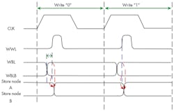
Figure 10 shows a simulated write timing diagram for the 10T SRAM cells. The write timing design must ensure that the data on write bit-line pairs is stable before the write word-lines turn high, which can reduce energy consumption of memory during a write operation.
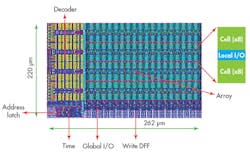
Figure 11 depicts layouts for the 16-kb 10T SRAM and 8T SRAM cells as fabricated in a 65-nm process technology. The 10T SRAM has an area of 262 × 220 µm2, while the 8T SRAM measures 302 × 102 µm2. The 10T SRAM allows for a 38% area overhead to account for array circuits.
Simulation Results
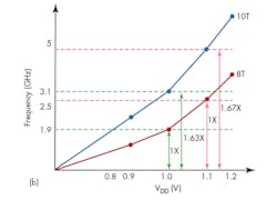
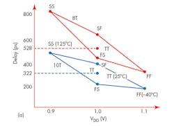
To obtain an operating frequency for the memory circuits, simulations were performed with HSPICE from Synopsys. Figure 12 shows the output data delay of 10T SRAM and 8T SRAM from the clock rising edge under five technology corners (TT, FF, FS, SF, and SS), and the characteristics of the operating frequency when supply voltage is changed. As illustrated in Figure 12, the output delay of the 10T SRAM is reduced by 39% compared with the 8T SRAM, and the frequency increases by 1.63 times under the TT technology corner.
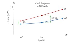
Figure 13 compares the power consumption for the 10T SRAM and 8T SRAM approaches. The power consumed in the 10T SRAM is 30.4% lower than the 8T SRAM at an 800-MHz operating frequency under the TT corner.
In summary, the proposed 10T SRAM design provides a 38% area advantage compared to an 8T SRAM approach. It achieves a much greater SNM than the 8T SRAM cell for a +1.0-V dc supply, with the output delay of the 10T SRAM design reduced by 39% compared to the 8T SRAM cell. Also, power consumption for the 10T SRAM design reduced by 30.4% compared to the 8T SRAM cell design.
This file type includes high resolution graphics and schematics when applicable.
Acknowledgment
This work was supported by the Educational Commission of Hunan Province (grant No.09C886).
Xu Jianming and Peng Xuhong are with the Department of Information Engineering, Shaoyang University, Shaoyang 422000, People’s Republic of China; e-mail: [email protected].
References
1. International Technology Roadmap for Semiconductors 2005, http://www.itrs.net /Links/2005ITRS/Home2005.htm.
2. Seyab Khan and Said Hamdioui et al, “Trends and Challenges of SRAM Reliability in the Nano-scale Era,” International Conference on Design & Technology of Integrated Systems in Nanoscale Era, 2010, pp. 1-6.
3. Yen Hsang Tseng, Yimeng Zhang, Leona Okamura, and Tsutomu Yoshihara, “A New 7-Transistor SRAM Cell Design with High Read Stability,” International Conference on Electronic Device, Systems, and Applications (ICEDSA), 2010, pp. 43-47.
4. Azeez J. Bhavnagarwala et al., “The Impact of Intrinsic Device Fluctuations on CMOS SRAM Cell Stability,” IEEE JSSCC, Vol. 36, No. 4, April 2001, pp. 658-665.
5. D. Burnett, K. Erington, C. Subramanian, and K. Baker, “Implications of fundamental threshold voltage variations for high-density SRAM and logic circuits,” in Proceedings of the Symposium on VLSI Technology, June 1994, pp. 15-16.
6. G. Sery et al., “Life is CMOS: Why Chase Life After?,” Proceedings of the IEEE Design Automation Conference, June 2002, pp. 78-93.
7. Y. Morita et al, “An Area-Conscious Low-Voltage-Oriented 8T-SRAM Design under DVS Environment,” Digest of Technology Papers, 2007 Symposium on VLSI Circuits, pp. 256-257.
About the Author
Voice Your Opinion!
To join the conversation, and become an exclusive member of Electronic Design, create an account today!

Leaders relevant to this article:
