11 Myths About NAND Flash

This file type includes high-resolution graphics and schematics when applicable.

NAND flash has become the de facto memory standard in the years since Toshiba first introduced it almost three decades ago. However, many misconceptions remain to this day about its use. A wide variety of NAND flash-memory products are available, all with significantly different features and capabilities. From single- and multi-level cell to 3D and more, the diversification of NAND flash has design engineers weighing their options—and asking questions.
Think you know NAND flash? Let’s take a look at some common misconceptions about this important technology.
1. All NAND flash has the same interface.

NAND flash, introduced by Toshiba more than 20 years ago, is available in both the asynchronous and toggle-mode interfaces. The original asynchronous interface is found mostly in lower-density devices (<32 Gb), while high-density NAND flash (≥64 Gb) is typically used in the toggle-mode interface. While most of the signal lines are the same between the two interfaces, the toggle-mode interface adds a DQS (data/output/strobe) pin that’s used for high-speed data transfers.
2. UFS memory is primarily just for smartphones.
With Embedded MultiMediaCard, or e.MMC, smartphones were a key driver for adoption, but the breadth and variety of applications soon exploded to include tablets, games, e-readers, cameras, streaming-media devices, printers, servers, wearable devices, automotive infotainment, and more. Likewise, for Universal Flash Storage (UFS), while smartphones are driving significant growth, many of the same applications that adopted e.MMC are now starting to adopt UFS into their designs to take advantage of its higher performance.
Essentially, any application needing high-density embedded memory with fast performance can be a candidate for UFS. The availability of host processors that support UFS continues to expand.
3. e-MMC and UFS aren’t suited for automotive.
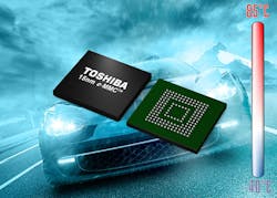
The memory-storage requirements for automotive continue to increase, especially due to the growing connectivity in vehicles and advances in autonomous driving capabilities. Entertainment, maps, driver-assist functions and more all require more memory storage, which is the bailiwick for embedded memory such as e.MMC (Fig. 1). Likewise, automotive will adopt UFS because it brings enhanced performance.
4. All NAND flash requires the host to implement error correction code (ECC).
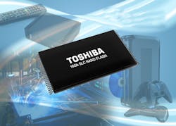
If the host processor doesn’t have a built-in ECC engine, it’s still possible to use NAND flash. While plain or raw NAND devices require the host to implement ECC, many NAND flash products feature built-in error-correction capability like serial NAND, e.MMC, UFS, and BENAND (Toshiba’s SLC NAND with built-in ECC, see Fig. 2).
5. Data in NAND flash always lasts at least one year.
The data retention of NAND flash comes down to four main factors: the temperature, the number of write/erase cycles to a block, the ECC, and the type of memory cell—e.g., single-level cell (SLC), multi-level cell (MLC), or triple-level cell (TLC). While the nominal data-retention specification for NAND flash is one year, that’s only when at a specific temperature, write/erase cycle limit, and ECC requirement. The write/erase cycle limit is different for SLC, MLC, and TLC devices, as well as the ECC.
6. NOR flash is for code storage and NAND flash is for data storage.
This was once the basic rule of thumb because NOR flash had faster random-access speeds for reading and NAND flash had lower bit cost and faster programming speeds. Microcontrollers executed random code from NOR flash via a separate address and data bus.
This process is more nuanced in today’s systems, though. Modern processors began to eliminate the parallel address/data bus due to the high pin count, and NOR flash has instead migrated to a serial interface. Now, code is often shadowed (copied) from NAND flash-based storage (e.g., NAND or e.MMC) to DRAM for execution.
7. UFS will never surpass e.MMC demand, but if it does, e.MMC will quickly go away.
UFS is quickly being adopted by high-end smartphones, including many models launching this year, and will migrate to mid-tier phones soon after. To fully take advantage of the UFS-supported faster interface, UFS is primarily targeted for densities of 32 GB and higher, since fast sequential write speeds are enabled by interleaving multiple NAND die, which can only cost-effectively be implemented at higher densities.
Densities such as 4, 8 and 16 GB will continue to be supported with e.MMC, as many applications require these lower densities, and densities of 32 to 128 GB+ will migrate to UFS over time. The market demand for UFS will eventually surpass e-MMC over the next couple years, though e-MMC will continue to remain in the market beyond that for applications requiring lower densities.
8. Once detecting the initial factory-marked bad blocks and making sure they’re not used, one needn’t worry about bad blocks anymore.
There will be a few blocks that fail over time—sometimes called grown bad blocks. While the percentage of good blocks that fail before the maximum number of write/erase cycles is low (on the order of 0.1%), since the number of grown bad blocks is not zero, the flash-management software must be able to retire blocks.
9. SLC NAND flash is rated for 100k write/erase cycles and MLC for 10k write/erase cycles.
While these were the specifications of NAND flash years ago, this is no longer accurate since many lithography generations have passed. Typical SLC NAND flash has an endurance of 50-60k cycles (24-nm generation) and MLC NAND flash has an endurance of 3k cycles (15-nm generation).
10. Everyone that makes NAND flash follows the ONFi standard.
The Open NAND Flash Interface (ONFi) standard was created by a consortium of companies that make NAND flash. However, Toshiba (the inventor of NAND flash), and Samsung never joined ONFi. The Joint Electron Device Engineering Council (JEDEC) has since unified the Toshiba/Samsung toggle-mode standard and the ONFi standard, so there’s now good compatibility for modern NAND devices.
11. NAND flash is only available in the parallel asynchronous or toggle-mode interface.
There are now multiple manufacturers making serial interface NAND flash; more specifically, SPI (serial peripheral interface). This follows the trend of microcontroller manufacturers eliminating the high-pin-count parallel address/data bus in favor of lower-pin-count interfaces.

About the Author

Scott Beekman
Vice President, Memory Business Unit, Kioxia
Scott Beekman is Vice President of the Memory Business Unit at Kioxia.

Doug Wong
Senior Member, KIOXIA Technical Staff
Doug Wong is a Senior Member of the Technical Staff at KIOXIA America, where he has contributed to the advancement of memory technologies since 1993. He began his career with KIOXIA in the company’s Memory Division (then part of Toshiba America) and has since focused on a broad range of memory solutions, including PSRAM, SRAM, MROM, EPROMs, NOR flash, and NAND flash.
Doug has been an active contributor to industry standards as a member of the JEDEC JC42.4 committee since 1996. He holds a Bachelor of Science in Electrical Engineering from California Polytechnic State University San Luis Obispo and a Master of Science in Electrical Engineering, with a focus on solid-state physics, from UCLA.
Comment About the Article
To join the conversation, and become an exclusive member of Electronic Design, create an account today!

Leaders relevant to this article: