This file type includes high-resolution graphics and schematics when applicable.
Over the past couple of decades, the solid-state drive has evolved from a very expensive niche-market storage device to a mainstream storage option in client PCs, enterprise servers, and consumer electronics. They come in many different form factors and interfaces, but all have essentially the same architecture. This article digs into the basics of what makes a solid-state drive tick.
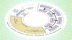
A SSD has three main components: the controller (including firmware) and the NAND memory (Fig. 1). Together, these components determine the ideal systems for the SSD, its reliability, and how much it will cost.
Controller and Firmware
The controller, a key part of every SSD, gives the drive its personality. Its main function is to provide a standard interface that allows for communication between the host system and SSD. Most industry-standard form factors, such as SD cards, CompactFlash cards, 2.5-in. SATA SSDs, and the like, call out specifically what interface the controller must support.
Several of the most common interfaces are IDE/PATA, SD, SATA, and USB. Many of these interfaces were originally created for rotating hard-disk drives. Instead of creating a completely new standard for flash-storage interface, most SSDs today just leverage existing hard-drive standards. The controller in the SSD has the principal task of emulating these standards and making the SSD appear as a standard mass-storage device transferring in blocks, sectors, or other standard “chunks” of data.
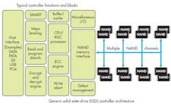
In addition to its host-interface function, the controller must also manage the flash-memory components. There are as many different configurations of controller and NAND flash architecture as there are purposes for a SSD (Fig. 2).
On simple flash cards, the need may arise for a single channel between the controller and a single memory component. On advanced SSDs for enterprise systems, there can be many channels (in some cases as high as 10 or more) that stripe across the NAND components. This striping allows for simultaneous reading and writing of the NAND memory, thereby creating greater overall data-transfer performance.
Almost every controller has firmware. You can think of it as the operating system of the SSD. While some functions, like ECC, are hard-coded into the SSD silicon, most are controlled by the firmware.
Firmware can be readily modified to add or remove features, compensate for deficiencies in the latest batch of NAND, or meet a certain host-system requirement. Some SSD manufacturers allow for field updates of firmware, while many lock firmware in at time of manufacture.
For industrial applications, many embedded-system OEMs prefer to have a SSD with locked-BOM and firmware, which never changes. Thus, their initial qualification is still valid throughout the life of the product.
NAND Flash Memory
Almost all SSDs today are made with NAND flash memory, although officially a “solid-state” drive could be made from other semiconductor memory such as DRAM, SRAM, etc. NAND has become the de facto standard, since it’s non-volatile (retains data after power is removed) and provides a great cost per megabyte compared to other memory technologies.
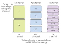
NAND comes in several different varieties, which are key determining factors in the reliability and expense of the SSD. The three main types of NAND flash are SLC, MLC, and TLC (Fig. 3):
• Single-level cell (SLC): One bit per cell; highest reliability, endurance, and data retention.
• Multi-level cell (MLC): Two bits per cell; medium reliability, endurance, and data retention.
• Tri-level cell (TLC): Three bits per cell; lowest reliability, endurance, and data retention.
In the case of SLC NAND, the first NAND variety on the market, each cell is divided to represent either a low or a high. Storing a bit in a SLC NAND cell is only a matter of setting a low or high voltage. Retrieving that bit is as simple as determining if the cell contains a low or a high voltage. There’s plenty of guard band to play with, making a highly reliable design—especially when extreme environments, noise, and wear level are taken into account.
Over time, engineers saw an opportunity to increase storage from a single NAND cell by storing more than a single bit. They did this by varying the voltage level in the cell. By creating four distinct voltage states that could be accurately set and retrieved, two bits can be stored. The binary representation of these states is 00, 01, 10, and 11.
This version of NAND, which stores two bits, was called multi-level cell, or MLC, NAND. Even though the “multi” in MLC denotes two or more bits per cell, in practice it only refers to the two-bit-per-cell variety.
With two bits per cell accomplished, the race was on to store more bits per cell. While it seems like a pretty straightforward objective, it’s actually much more complicated to accomplish. The end product must reliably operate within some minimal level of usefulness over a period of time.
After a number of years, the tri-level cell was brought to the market. This requires the NAND cell to store eight distinct states (000, 001, 010, 011, 100, 101, 110, 111) in the same area where SLC only has to store two. It brings down the guard band between states and limits the reliability and endurance of the NAND flash itself.
Nonetheless, this is an amazing accomplishment and enables new price points for flash storage. Controllers with sophisticated firmware are needed to make TLC memory useful for lower-duty-cycle applications such as consumer flash cards, USB flash drives, and even enterprise SSD when used as a disposable cache.
The NAND varieties described above are called planar NAND. They represent one layer of memory on the silicon. There’s a new, emerging technology making waves called (depending on the manufacturer) 3D or Vertical NAND. It essentially stacks multiple layers of SLC, MLC, or TLC NAND cells on a single piece of silicon during the manufacturing process.


