Embedded memories and logic libraries support many low-power design techniques that today’s system-on-chip (SoC) designers can use to reduce power dissipation while still meeting area and performance targets. Since low power is a requirement for both mobile and enterprise class chips, high-speed and low-speed libraries and memories need to support low-power design techniques.
Related Articles
- Fundamentals Of Low-Power Design
- Understanding Low-Power IC Design Techniques
- Low-Power Design Enables PoE Networking
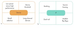
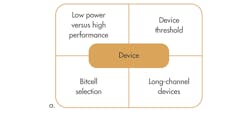
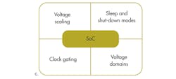
Low-power architectural choices like the low-power MIPI M-PHY interconnect1 and the L1 state of the PCI Express interface2 are available. Low-power libraries and memories are essential in implementing these options, which can be divided into three categories: device-level techniques, IP-level techniques, and SoC-level techniques (Fig. 1).
Power Components
Dynamic and leakage power are important concerns in most SoC implementations. While designers of chips targeted at mobile markets worry about leakage, they also look to keep dynamic power in check. The total power dissipated on an SoC can be broken down into dynamic power and static power. The well-known equation is:
Power = ½ a C*V2*f + V*ILeakage
In other words, reducing the components of dynamic power (C*V2*f) and static power (V*Ileakage) can reduce total power dissipation.
In addition to these architectural-level choices, low-power techniques should be adopted at the device, IP, and SoC levels to reduce total power dissipation.
This file type includes high resolution graphics and schematics when applicable.
1. Choose Thy Process Carefully
Designers should choose the process variant available that is most conducive to power reduction. The typical choices are between a higher-speed, higher-leakage process variant and a slower but lower leakage process variant with a higher nominal voltage. Depending on the target market, a different choice may be appropriate.
For mobile and handheld applications, where most of the energy is consumed in standby mode, the low leakage process is preferable. While leakage is still an important consideration for many non-mobile chips, reducing dynamic power is the primary goal for networking and high-performance computing chips. These enterprise class chips can address the leakage component by shutting off different sections of their SoC, so a high-speed process with a lower operating voltage is the appropriate choice for these applications.
A FinFET process offers much lower leakage than the equivalent planar process, but it is more expensive. Although the gate capacitance is higher in the FinFET process, the lower leakage and nominal voltage makes it a much lower-power choice.
2. Thou Shalt Raise Thine Threshold
Using higher-threshold devices is a well-documented technique to reduce leakage. Providing footprint-compatible cell libraries with multiple VT options allows them to be used in an optimal distribution to obtain the lowest leakage implementation while still hitting the performance targets.
3. Thou Shalt Increase Thine Channel Lengths
In addition, using devices with different channel lengths can help reduce leakage while achieving performance targets. Devices with longer channel lengths have lower performance but also lower leakage. Compared to the higher-threshold devices, longer-channel transistors also have nominally larger cell area but superior performance.
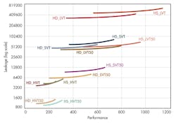
A longer-channel device with a lower threshold is a better choice than the minimum channel-length device with higher threshold (Fig. 2). Implementation tools must have access to libraries with a variety of channel lengths to automatically make these optimizations.
Even though the cells themselves are larger than the corresponding minimum-channel versions, longer-channel cell libraries deliver less area at the module level mainly because they deliver higher performance than higher-threshold devices. In other words, a long-channel standard Vt (SVt) device not only may reduce leakage more than the equivalent minimum-channel length and high Vt (HVt) device, it also will deliver higher performance and a smaller area implementation.3
4. Choose Thine Bitcells With Care
Since memory is a big component of the total SoC power dissipation, it’s important to consider the choice of bitcells. Luckily, the choice here is straightforward: smaller bitcells have lower leakage but also have lower performance than larger bitcells. SoC designers can select the bitcell that will enable them to meet their performance target.
5. Thou Shalt Split Your Bitline Capacitance
While the choice of bitcell affects leakage and area, the way in which the actual memory is architected impacts the dynamic power as well. The bitline capacitance is the single largest switching capacitance in a typical memory. So banking, wherein the bitline is split into smaller portions, is a good technique to reduce dynamic power. Where applicable, splitting the wordline capacitance also helps to reduce dynamic power dissipation. The added benefit of these techniques is a faster memory access time (clock to q), but it comes with increased area.
6. Bias Your Array Or Else…
Array biasing is a well-proven technique to reduce leakage when the memory is not being accessed. Unlike body biasing, which uses gate biasing, array biasing uses source biasing to reduce the leakage. Controlling the level of biasing allows the memory to retain its contents while still providing better leakage results. Innovative methods can be used to ensure a very fast wake-up time from this mode. Designers of large memory have used these methods to source bias unused portions of the array into a “sleep” mode while still allowing access to the memory.
7. Thou Shalt Split Your Power Rails
Since operating voltage is such a major factor in power consumption, reducing the voltage is a key technique in reducing power. However, most foundry bitcells limit the bitcell operating voltage range to only 10% less than the nominal voltage. In such a case, it is useful to have the periphery run on a lower voltage level than the supply to the bitcell array. To be most effective, it is important that a wide differential (at least 250 mV) is supported between the periphery and bitcells. To make this happen, memories should have integrated level shifters.
8. Flip-Flops Of The World, Unite
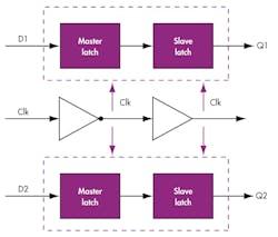
Using multibit flip-flops is an effective way to reduce clock switching power. Now fully supported in mainstream EDA flows, they reduce the number of individual loads on the clock tree and thus the overall dynamic power. Area and leakage power savings also result from sharing the clock inverters in the flip-flops (up to 50% for a dual flip-flop) (Fig. 3).
9. Voltage & Frequency Scaling
The dual-rail technique discussed earlier is part of a greater SoC-level design technique commonly known as voltage scaling. The idea is to operate the SoC at the minimum voltage required to deliver the instantaneous performance required for the application at hand. For example, for the optimal power consumption, higher voltages are used when higher frequencies are required, and lower voltages are used when lower frequencies are required.
10. The Sleepy & The Shutdown Shall Inherit The Earth
There are times when the application doesn’t need to access memory instances or whole modules of the SoC. In such cases, those sections of the SoC can be shut down through the use of power gates. These modules could just be individual memory instances, in which case the power gates can be integrated into the memory. When these power gates “turn off” the power supply, the contents of the memory or other storage elements are lost.
A sleep mode is useful when the contents of the storage element need to be retained, whether it is a flip-flop or a memory. It’s important to implement retention flops for sleep modes in larger modules, and it is essential that these flops are in the logic library. In memory instances, the periphery may or may not be shut down, but the array voltage is effectively reduced to just above bitcell retention voltage. This can be done through reducing the power supply voltage or source biasing the array as described earlier.
11. Thou Art Thine Clock’s Gater
When the largest switching capacitance is the clock tree, it makes a lot of sense to start gating clocks when blocks are not in use. This dramatically reduces the dynamic power consumption of the SoC. Wherever possible, integrated clock gating cells should be used to reduce dynamic power dissipation.
12. Divide And Conquer (The Voltage Domains)
When different parts of the chip run at different speeds, they can be run at different voltage levels. In such cases, well-crafted up- and down-level shifters in the library are essential to a successful SoC implementation. When the different voltage domains have voltage scaling implemented, the SoC designer also needs up- and down-level shifters to allow for voltage movement in both directions.
Summary
With power reduction the top challenge for many of today’s SoCs, designers need to use every possible tool and technique at their disposal. Often the importance of libraries and memories can be overlooked. A comprehensive library of low-power libraries and memories that support the 12 tenets described here is critical to achieving low-power requirements.
References
1. “The MIPI M-PHY Reduces Power In Mobile Chip-To-Chip Interfaces,” http://electronicdesign.com/power/mipi-m-phy-reduces-power-mobile-chip-chip-interfaces, Electronic Design, May 6, 2013
2. “Reduce Power In Computing And Memory Interfaces Without Impacting Performance,” http://electronicdesign.com/power/reduce-power-computing-and-memory-interfaces-without-impacting-performance, Electronic Design, October 23, 2013
3.Reducing Static Power in 40nm and 28nm Designs Using Multi-Channel Libraries, SNUG Silicon Valley 2011, Deepak Sherlekar
Prasad Saggurti is a senior product managerresponsible for embedded memory and test & repair intellectual propertyat Synopsys. Previously, heheld senior engineering and marketing roles at MoSys, ARM, National Semiconductor,and Sun Microsystems. Hehas an MSEE from the University of Wisconsin-Madison and an MBA from the University of California-Berkeley. He can be reached at [email protected].
About the Author
Prasad Saggurti
Senior Product Manager
Prasad Saggurti is a senior product managerresponsible for embedded memory and test & repair intellectual propertyat Synopsys. Previously, heheld senior engineering and marketing roles at MoSys, ARM, National Semiconductor,and Sun Microsystems. Hehas an MSEE from the University of Wisconsin-Madison and an MBA from the University of California-Berkeley. He can be reached at [email protected].
