The Active Clamp Flyback Converter: A Design Whose Time Has Come

This article is part of TechXchange: Power Supply Design
Download this article in PDF format.
One trend that shows no size of ending is the move to smaller personal electronic devices. From smartphones to tablets, each successive generation is smaller and more powerful than the last. It’s usually battery-powered and must be regularly charged by an external charger or adapter.
The movement to more powerful processors and larger screens poses a challenge for the power designer, who must continually come up with new ways to boost efficiency and reduce battery-charger size. Stringent new standards such as DoE Level VI and EU CoC V5 Tier-2 raise the efficiency requirements on a wide range of power adapters.
As a result, designers must improve the design of the discontinuous-mode quasi-resonant flyback topology. Such a converter is traditionally used to implement a low-cost ac-to-dc power adapter for power levels up to 100 W.
A flyback converter uses relatively few components, is simple to design, and can accommodate multiple outputs. With a silicon power MOSFET, its efficiency can run as high as 90% if synchronous rectification is employed and the switching frequency is kept below 100 kHz to reduce switching losses.
Sponsored Resources:

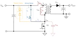
Figure 1 shows the essential elements of the flyback design. The transformer acts as a coupled inductor rather than as a true transformer. When the power switch is on, the flyback converter stores energy in the primary-side inductor. During the switch off time, the energy transfers to the secondary and from there to the output. Current flows in either the primary or secondary winding, but not both at the same time.
The simplest mode of operation is discontinuous mode (DCM). The power stage is designed to allow the transformer to demagnetize completely during each switching cycle. The most basic DCM control scheme switches at a fixed frequency and modulates the peak current to support load variations.
Stressed Out Transistor
One of the issues with the design shown in Fig. 1 is that the flyback topology imposes a high level of stress on the low-side switching transistor Q1 when it turns off. Let’s analyze this in a little more detail.
As shown in Figure 2, we can model the flyback transformer as a leakage inductance (LLK), a primary-side magnetizing inductance (LPM), and an ideal transformer. The leakage inductance is effectively in series with Q1. When Q1 switches off, the current through the LLK and LPM is interrupted. The energy stored in LPM transfers to the secondary winding and the output, but the leakage inductance energy causes a large voltage spike that stresses the power switch.
2. Dissipating the energy from the leakage inductance requires a passive or active clamp circuit. (Source: TI Training: “What is active clamp flyback?”)
Adding a clamp circuit (also called a snubber) on the primary side of the transformer provides a path for the leakage inductance current. The clamp design must meet several goals: it must limit the stress on Q1 to an acceptable level; it must discharge the leakage inductance quickly with minimum losses; and it must not degrade the overall loop dynamics.
Fig. 2 shows two options for the clamp. The passive clamp uses a Zener diode and a blocking diode in series. When Q1 is on, the blocking diode is reverse-biased and no current flows through the clamp. When Q1 turns off, the voltage spike turns on the diode, and the circuit clamps the drain voltage to (VIN + VZ + VD).
This method is simple and relatively inexpensive, but the passive clamp circuit lowers the system efficiency because it dissipates the leakage inductor energy as heat. The power loss increases with switching frequency according to the passive-clamp power dissipation equation:
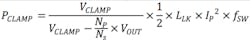
where VCLAMP is the voltage across the clamp when Q1 is off; NP/NS is the transformer turns ratio; and IP is the transformer peak primary current.
Once the leakage energy is depleted, the output diode continues to conduct until the magnetizing current has decreased to zero. After the output diode turns off, the residual energy in the system causes a resonance between the magnetizing inductance LM and the switch-node capacitance CSW.
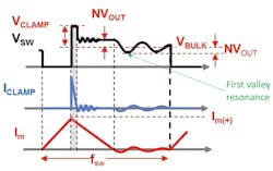
3. The QRF uses the first resonant valley to trigger the next switching cycle. (Source: Texas Instruments)
The quasi-resonant (QR) mode of operation (Fig. 3), also referred to as critical conduction mode (CCM) or transition mode (TM), takes advantage of this resonance to reduce losses. The QR flyback (QRF) controller detects the first resonant valley—when VSW is at a minimum—and uses the event to control the turn-on of the MOSFET for the next cycle. This technique is known as valley switching (VS).
QR is a popular choice for low-power flyback converters and delivers the maximum amount of power with the passive-clamp configuration. Since VSW is not zero, though, there’s still a switching power loss PSW(QRF), given by the equation:
Adding ZVS Eliminates Switching Loss
The active clamp circuit solves this issue. This design replaces the two diodes with a high-voltage FET (QC in Fig. 2) in series with a clamping capacitor. The FET can be either p-channel or n-channel. The p-channel device is simpler to control, but fewer choices are available at high voltages. For offline use, therefore, an n-channel FET is preferred, even though it requires a high-side driver.
Instead of wasting the leakage inductance energy, the active clamp circuit improves efficiency by storing the energy in a capacitor, then delivering it to the output later in the switching cycle. Combining TM operation with an active clamp can completely remove the switching loss, allowing the switching frequency of an active clamp flyback to be higher, thus reducing the size of the power supply (Fig. 4).
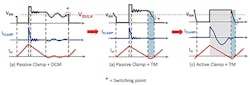
4. A comparison of three clamp strategies shows successively lower switching voltage as we progress from left to right. (Source: TI Training: “Comparison of GaN and Silicon FET-Based Active Clamp Flyback Converters - Part 1”)
During the demagnetization time of the transformer, the high-side switch remains on and the clamp capacitor resonates with the leakage inductor. This allows the active clamp to recycle the leakage energy to the output.
By keeping the high-side switch on, the magnetizing current Im is allowed to ramp all the way down to zero and past zero to the reverse direction; QC then turns off with a little bit of negative current flowing in it. The negative current discharges the junction capacitance of the switch node and allows the low-side switch to turn on with zero volts across it after a short delay. Thus, the active clamp flyback (ACF) operating in transition mode can also eliminate the switching loss. This technique is called zero-voltage switching (ZVS).
The ACF has two slight drawbacks, though. Building up the additional negative current increases the flux density, so the active clamp core loss is slightly higher than that of the passive clamp. Also, the clamp current flows in the transformer primary winding during demagnetization time. The larger primary current increases the total winding loss; a large amount of negative current can negate the efficiency gains of the ACF if the switch-node capacitance becomes too large.
The table compares the performance of the three topologies in four categories: clamp loss, switching loss, core loss and winding loss.

Improving the efficiency with an active clamp pays dividends in power density. Switching at 150-260 kHz, a 65-W passive clamp QRF can achieve a power density of around 11W/in.3; the equivalent active clamp flyback design switching at 120-165 kHz can achieve around 14W/in.3.
GaN Switching: The Icing on the Cake
Changing the silicon power devices to transistors based on gallium nitride (GaN) yields further efficiency improvements. Compared to a silicon MOSFET, a GaN device has lower on-resistance, higher breakdown voltage, better reverse-recovery characteristics, and can operate at higher temperatures. It also has much lower switching losses; therefore, it can operate at higher switching frequencies.
Higher switching frequencies allow for the use of smaller capacitors, inductors, and transformers, which in turn reduce power converter size, weight, and cost. Switching to GaN can cut the size of the adapter by up to 50%.
The TI Power Supply Design Seminar for 2018 includes a set of training videos with a detailed analysis of the active-clamp flyback circuit and a comparison of Si and GaN implementations.
Practical Implementation of the ACF with the UCC28780
Reliably controlling the active clamp high-side switch isn’t easy, but new devices such as the Texas Instruments UCC28780 simplify the task considerably. The UCC28780 is a high-frequency active-clamp flyback controller that monitors VSW and adjusts the on-time of QC for zero-voltage switching.
The device works with VDS-sensing synchronous rectifier controllers for higher conversion efficiency and a more compact design. A user-programmable advanced control law feature allows performance to be optimized for both Si and GaN primary-stage power FETs, enabling compliance with efficiency standards such as DOE Level 6 and COC Tier 2.

5. The UCC28780 simplifies the design of an ACF converter using either Si or GaN power FETs (Source: “UCC28780 High Frequency Active Clamp Flyback Controller” PDF, p. 37)
Figure 5 shows the UCC2870 in a typical off-line application. Tying the SET pin to either ground or REF allows the designer to select a GaN-based or a Si-based half-bridge power stage, respectively.
On the secondary side, Texas Instruments' new synchronous rectifier controller, the UCC24612, is specifically designed to work with the UCC28780, allowing the rectifier diode to be replaced with a more efficient FET.
Other advanced UCC28780 features include operation up to 1 MHz; adaptive ZVS with auto-tuning to compensate for component variations; active ripple compensation; adaptive burst mode to improve efficiency with light or medium loads; and programmable over-power protection providing consistent power for thermal design across a wide line range.
Figure 6 shows how a GaN-based UCC2870 design supplying 45 W exceeds the requirements of the new efficiency standards.
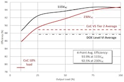
6. A 45-W, 20-V ACF design based on the UCC28780 and a GaN power stage comfortably exceeds the new efficiency standards. (Source: “UCC28780 High Frequency Active Clamp Flyback Controller” PDF, p. 1)
Texas Instruments has also developed a fully-tested ac/dc ACF power adapter reference design that delivers 65 W. The design combines the UCC28780, the UCC24612, and the TPS25740B, TI’s USB Type-C and USB PD source controller, to meet the USB Power Delivery (USB PD) version 2.0 standards. Operating at 600 kHz, the design achieves a peak efficiency of 92%. Measuring just 62 × 26.8 × 20 mm, its power density of 30 W/in.3 is much higher than traditional solutions.
In addition to those already mentioned, the block diagram (Fig. 7) shows the other key components. The main switching devices are NV6115 and NV6117 GaN devices from Navitas Semiconductor. Other devices include the ISO7710 reinforced single-channel digital isolator; the CSD17578Q3A 30 V N-Channel NexFET Power MOSFET; the ATL431 2.5V Low-Iq Adjustable Precision Shunt Regulator; and the TPD1E05U06 ultra-low-capacitance IEC ESD protection diode.
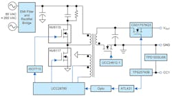
7. Shown is a block diagram of a USB PD-compliant 65-W adapter with 92% efficiency. (Source: TI Designs: TIDA-01622 PDF)
The design is suitable for a wide range of laptop adapters, smartphone chargers, and other consumer and industrial ac/dc applications.
Conclusion
The active-clamp flyback topology has long been recognized as a superior solution for small high-efficiency power adapters, but difficulties in implementation have prevented its widespread use. Increasing demands for compact, high-efficiency solutions have led to the development of integrated ACF controllers such as the UCC28780, which allow power designers to increase power density and meet new regulatory benchmarks.
Read more articles in TechXchange: Power Supply Design
Sponsored Resources:
About the Author
Paul Pickering
Paul Pickering has over 35 years of engineering and marketing experience, including stints in automotive electronics, precision analog, power semiconductors, flight simulation and robotics. Originally from the North-East of England, he has lived and worked in Europe, the US, and Japan. He has a B.Sc. (Hons) in Physics & Electronics from Royal Holloway College, University of London, and has done graduate work at Tulsa University. In his spare time, he plays and teaches the guitar in the Phoenix, Ariz. area
Comment About the Article
To join the conversation, and become an exclusive member of Electronic Design, create an account today!

Leaders relevant to this article: