The Charge-Pump Option to LDO and Inductor-Based Regulators
Download this article in .PDF format
A charge pump is a type of switch-mode power-supply (SMPS) circuit that’s used as a dc-dc converter or regulator with appropriate feedback control. The charge pump is often overlooked when considering a new design requiring these circuits. Because of its simplicity and other benefits, the charge pump may be a better choice over the use of a low-dropout (LDO) linear regulator or a switch-mode regulator using an inductor. In your next design, you may want to consider this classic circuit and its advantages.
Charge-Pump Basics
The basic charge-pump circuit is a switch-mode dc-dc converter that’s often needed in designs requiring more than one dc supply voltage. It’s made up of switches and capacitors. The switches are usually diodes in discrete designs, but are also MOSFETs in IC versions. The capacitors are electrolytics or ceramics depending on the switching speed. There’s no need for an inductor.
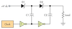
Figure 1 shows the basic charge pump that’s connected as a voltage doubler. The operation is a two-step charge-discharge cycle where “flying” capacitor C1 charges then discharges into C2. When the clock drives the output of inverter 1 low, D1 is forward-biased, charging C1 to V dc. D2 is off at this time. Then the clock drives the output of inverter 1 high to V dc.
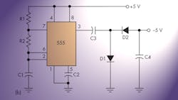
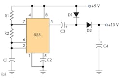
Figure 2 shows some examples of discrete charge pumps using the popular 555 timer IC. Figure 2a is a voltage doubler. The 555 timer operates as an astable multivibrator with a frequency set by R1, R2, and C1. The rectangular wave output at pin 3 switches from +5 V to near ground. When pin 3 is low, C3 charges through D1 to +5 V. When pin 3 goes to +5 V, D2 conducts, connecting the +5 V from the timer in series with the +5 V on C1, thereby charging C4. The output is +10 V, less the diode drops.The charge on C1 is now in series with V dc from inverter 1. The output of inverter 2 is low, so D2 is forward-biased and C2 charges to 2 V dc. The output across the load is 2 V dc, less the diode forward drops, and any losses in the inverters. Schottky diodes are preferred because of the lower forward-voltage drops and high switching speeds. Clock speeds can be anywhere in the 10-kHz to 2-MHz range. If more diode and capacitors segments are added, the voltage can triple or quadruple (or even higher).
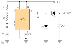
The charge pump can be configured as a voltage inverter, as seen in Figure 2b. With pin 3, the +5-V C3 capacitor charges through D1. When pin 3 goes to ground, D2 is forward-biased and C3 discharges into C4. Here, the +5-V supply is converted into an output of about –5 V, less the diode drops. Such an inverter circuit is useful when there’s a need for a negative supply. An example is when plus and minus supplies are needed for an op amp.
All charge pumps are some mix of switches and capacitors. Most integrated charge pumps use MOSFET switches with a low on-resistance and an integrated clock. The capacitors are always external to the IC so that the type and size may be selected according to the clock speed and the ripple requirements. The circuit may or may not be regulated.
Figure 3 shows some common configurations used in IC charge pumps. The switches are MOSFETs—switches S2 and S3 switch together, as do S1 and S4. The internal oscillator drives the switches.
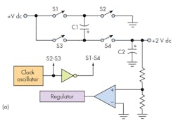
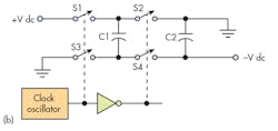
Fig. 3a shows the classic voltage-doubler configuration. With S2 and S3 closed and S1 and S4 open, “flying” capacitor C1 charges to the input voltage V dc. On the next half of the cycle, S2 and S3 open while S1 and S4 are closed. C1 is connected in series with the input voltage, and the combination charges C2. The output is 2 V dc, less the MOSFET drops. Note the feedback voltage divider that provides the regulation.
An inverting version is shown in Fig. 3b. With S2 and S3 closed and S1 and S4 open, “flying” capacitor C1 charges to the input voltage V dc. On the next half of the cycle, S1 and S3 open while S2 and S4 are closed. C1 discharges into C2. With the upper end of C2 grounded, the output at the other end is –V dc.
Typical Applications
Charge pumps are ideal for designs that use a larger, main single-voltage power supply that supplies most of the power but requires lower-current auxiliary voltage sources. Today, many ICs and components require multiple voltages. These can often be generated with a charge pump.
A classic example is the MAX232 charge-pump IC that generated the ±3- to 25-V supplies required to power the popular RS-232 serial interface line driver and receiver ICs from a 5-V supply. Another example involves the need to power a USB transceiver from a lower-voltage battery supply. TFT-LCD bias supplies represent one more example.
Some microprocessors require an auxiliary supply, as do many EEPROMs and flash memories. Most use on-chip charge pumps to provide these additional voltages.
The Benefits and Downsides of Charge Pumps
A charge pump holds some key advantages over other major types of dc-dc converters and regulators:
• Simplicity.
• Low cost. Fewer components. No inductor.
• Smaller PCB space. No inductor. Less height.
• Higher efficiency than linear. Estimated 20% improvement.
• Available in buck, boost, and inverting configurations.
• Multiple IC vendors.
Nothing is perfect for every design but the disadvantages of charge pumps are few:
• Best for small loads (< 200 mA).
• Electromagnetic interference (EMI). It is still a switch-mode circuit, so it generates some EMI.
• Less efficient than inductor-based designs.
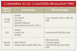
Comparing the Alternatives
When designing a product, your dc-dc converter and regulator choices are the charge pump, LDO and inductor-based switch-mode circuits. The table summarizes the advantages and disadvantages of each.
Design Notes
For discrete designs, Schottky diodes are a must for fast switching and lower voltage drops (0.2 to 0.4 V). In terms of capacitors, electrolytic or tantalum can be used for lower-frequency switching. However, their high equivalent series resistance (ESR) makes the circuit less efficient.
For IC designs, low-ESR surface-mount ceramic capacitors are essential for best efficiency. Sizes vary with switching speeds. Electrolytics or tantalums should not be used because of their high ESR. Some ICs may also cause polarity reversal during operation and many cause damage. Follow the recommendations of the IC manufacturer.
About the Author

Lou Frenzel
Technical Contributing Editor
Lou Frenzel is a Contributing Technology Editor for Electronic Design Magazine where he writes articles and the blog Communique and other online material on the wireless, networking, and communications sectors. Lou interviews executives and engineers, attends conferences, and researches multiple areas. Lou has been writing in some capacity for ED since 2000.
Lou has 25+ years experience in the electronics industry as an engineer and manager. He has held VP level positions with Heathkit, McGraw Hill, and has 9 years of college teaching experience. Lou holds a bachelor’s degree from the University of Houston and a master’s degree from the University of Maryland. He is author of 28 books on computer and electronic subjects and lives in Bulverde, TX with his wife Joan. His website is www.loufrenzel.com.
Comment About the Article
To join the conversation, and become an exclusive member of Electronic Design, create an account today!

Leaders relevant to this article: