As the markets for low-power near-field communications (NFC), radio-frequency identification (RFID), and advanced sensors expand, the need for smaller, lower-power, embedded non-volatile memory (NVM) increases. To successfully select and incorporate advanced NVM technology into these designs and meet evolving system demands, system architects and designers need to become more familiar with NVM intellectual property (IP) and understand how it impacts the key power, area, and reliability requirements of these markets. This is not easy because the requirements are quickly changing.
This file type includes high resolution graphics and schematics when applicapable.
Importance Of Endurance In Sensor Systems
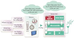
Real-time data logging is more prevalent than ever. From measuring your blood pressure to real-time stress on a steel bridge, sensor networks are quickly driving a new age of data collection, aggregation, and analysis, all requiring higher endurance (the number of times the NVM can be programmed/reprogrammed) in low-power multiple-time programmable (MTP) NVM.
Related Articles
- Controllers Speed NVM Express Drive Delivery
- NVM Express Delivers PCIe SSD Access
- NVM Express Changing The SSD Landscape
A sensor system’s requirements depend on how much MTP memory is needed and how often the data needs to be written (Fig. 1). The answers not only affect area and power (e.g., a large memory generally takes more power), they also drive the endurance and retention tradeoffs of the NVM.
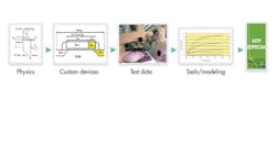
To meet endurance requirements, designers must use IP that starts with the fundamentals of physics, electron transfer, and storage and then innovates with custom devices, leading-edge tools, and state-of-the-art design (Fig. 2). Developing smaller, lower-power MTP NVM requires expertise in how charge is transferred during program and erase cycles. This expertise is necessary to optimize performance over different manufacturing materials and layout through monitoring voltage, current, and manufacturing level stressors during the development process.
When most people think about power, they focus on battery life, but power decisions also affect system area and dynamic performance. In the case of RFID tags, reducing power consumption increases the distance that you can read the tag from and decreases the size of the antennas. Reducing power can also shrink system area, cutting costs and enabling a wider range of packaging options.
For example, NFC tags are about the size and weight of a sticker and can be programmed thousands of times. Without small, low-power MTP NVM, this would never be possible. For Internet of Things (IoT) applications such as wearable computing, power consumption will impact the size of the battery, which could be a major factor in the technology’s adoption rates.
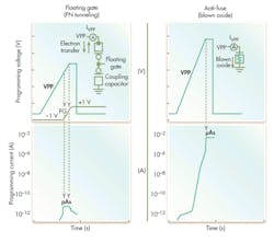
When choosing NVM for a low-power application, a good place to start is by learning a few basic principles of the technology that is used in the NVM development. Higher-density memories will typically require higher peak and average currents. NVM programming mechanisms (e-injection, blown gate, Fowler-Nordheim or FN tunneling, etc.) differ in currents as well. Figure 3 illustrates some fundamental differences between two popular programming mechanisms that can affect supporting circuits and total area of the NVM. As depicted here, a floating gate using FN tunneling requires less peak voltage and current to program data than the anti-fuse blown oxide method.
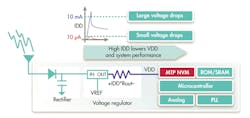
In addition, there are system-level concerns where the choice of NVM technology and density may negatively impact other components. Applications that deal with high-impedance supplies must take care that peak currents don’t dynamically push their system VDD outside the operating range of other on-chip components. At the system level, physically larger voltage regulators and batteries can be used to counteract high currents, but may have a negative impact on product size, cost, and performance.
For low-power designs, making the right NVM choice is critical. Designers should consider:
• How does NVM performance affect other components in the system? Does it cause other components to grow or shrink in area and power?
• What tradeoffs can be made in the system design? Which is more important, peak current or average current? How often will the system read from or write to the memory? (Will read current or write current cause the biggest system impact?) Can the system read at a lower speed to save power?
• What is the system-level impact (area and power) of higher-density or lower-density NVM solutions? Can a small amount of MTP/NVM + ROM be used? Is a large amount of MTP/NVM needed?
Trusting Your NVM IP Solution
End users typically don’t think about the NVM that enables reliable storage of passwords, GPS settings, and more. They implicitly trust it. This makes it even more important for product developers to not only compare the specifications for NVM with the system requirements, but to also consider additional factors when selecting an NVM IP supplier:
• Supplier’s history of growth and adaptation to changing markets
• Supported manufacturing options
• Supported quality levels (e.g., commercial, industrial, and automotive)
• Data retention—will the supplier still be around in 10 or more years?
DesignWare MTP NVM IP
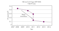
Synopsys first productized its 180-nm DesignWare MTP NVM IP in 2003. Since then, the company has continually focused on reducing power and area. Recently, Synopsys reduced its NVM IP area and power by more than 50% over previous generations. Figure 5 illustrates the continuing area reduction in the 180-nm node for 1-kbit MTP NVM.
Close collaboration with customers is critical to identifying and developing additional enhancements to NVM IP. With DesignWare NVM IP, architectural changes were made to the bitcell and high-voltage circuitry to minimize area and capacitive loading, as well as reduce analog and digital complexity. Also, internal drivers for slew rate control were tuned to reduce peak and average power and high-voltage circuits.
Conclusion
The increasing availability of more advanced, smaller, low-power NVM IP is enabling a broad range of new applications. Knowing how NVM IP impacts system power, area, and reliability in these applications is important to ensuring that the appropriate NVM IP has been selected.
This file type includes high resolution graphics and schematics when applicapable.
Troy Gilliland is a senior R&D manager for DesignWare Embedded Non-Volatile Memory (NVM) IP at Synopsys. Prior to joining Synopsys, he worked for VirageLogic, Impinj and Zilog in NVM, high-voltage, PLL, ADC, and RF mixed-signal development. With more than 17 years of experience in the semiconductor industry, he has strong knowledge of NVM/analog/mixed-signal and device physics. He holds both a BSEE and MSEE from the University of Washington, Seattle. He can be reached at [email protected].
