Designing Ultra-Low-Power Sensor Nodes for IoT Applications
Download this article in .PDF format
In many Internet of Things (IoT) applications, minimizing power consumption is a key design requirement. IoT capability involves adding sensors and connectivity to a valve or similar device in a location that may not already have power available. It’s often not feasible to add wiring, so a battery-operated solution is a preferred option.
In fact, sometimes it’s the only option. In cold-chain logistics, temperatures must be controlled at all times during shipping to prevent product deterioration. Vaccines, for example, may lose their efficacy or become toxic after even a short temperature excursion. To ensure product safety, it’s important to have a record of temperatures during the trip from factory to end user: A battery-powered data-logger records a time-stamped log of temperature variations, waking up periodically to take measurements.
Requirements of a Low-Power Node
In the home and on the farm, a common function of a sensor node is to track environmental data, such as temperature and humidity, which changes very slowly. To maximize battery life, the sensor node typically spends most of its time in a low-power “sleep” mode, waking up periodically according to a fixed schedule. During the waking period, the node gathers data and transmits it wirelessly to a central hub. Then it goes back to sleep until it’s time for the next measurement.
The Function of a Nano-Timer
It’s particularly important to minimize power consumption during the sleep phase, where the node spends the vast majority of its time.
A nano-timer can play an important role in minimizing sleep current and managing the go-to-sleep and wakeup phases of a battery-powered IoT node. This device increases battery life by replacing the internal timer of the microcontroller (MCU) with an analog device that consumes much less power. A nano-power system timer can wake up the MCU with an interrupt, or initiate sleep mode by completely shutting off power to the system.
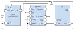
An application block diagram of the TPL5110 nano-timer is shown in Figure 1. The nano-timer controls the power supply to the MCU using a FET load switch. The TPL5110 can provide timing intervals between 100 ms to 7200 s; the interval is selectable via an external resistor. The MCU indicates completion of the data-gathering and transmission via a digital signal to the TPL5110’s “DONE” pin.
The nano-timer family has several family members, each with slightly different specifications. Consult the TI website for more information.
A Low-Power Wireless Sensor Node Design
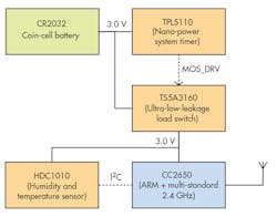
Figure 2 shows the system block diagram of a wireless IoT node using the TP5110. The design can achieve a battery life of greater than 10 years using a CR2032 lithium-ion coin-cell battery, which is widely available, low cost, and outputs a constant voltage practically until end of life.
The power-management block consists of the CR2032 coin cell and a TPL5110 driving a TS5A3160 ultra-low-leakage switch. The TPL5110 turns on the TS5A3160 to power on the system until the MCU signifies completion.
The other system components include:
• CC2650 wireless microcontroller (MCU): This MCU is designed for low-power, 2.4-GHz RF applications such as Bluetooth Low Energy (BLE), ZigBee, 6LoWPAN, and ZigBee RF4CE. The main processor is a 32-bit ARM Cortex-M3 running at 48 MHz. The peripheral set features an ultra-low-power sensor controller for the autonomous collection of analog and digital data, and an RF core with a separate ARM Cortex-M0 processor.
• HDC1010: This digital humidity sensor with integrated temperature sensor features a relative humidity accuracy of ±2% and a temperature accuracy of ±0.2°C, an I2C serial interface, and extremely low power consumption—it averages 1.2 μA at a measurement rate of one sample per second.
Adding the TPL5110 to the design reduces power consumption compared to using the CC2650’s internal sleep modes. That’s because the nano-timer consumes only 35 nA, compared to the 1-µA sleep mode of the CC2650.
For one measurement per minute, the off-state current consumption of this design averages 4.04 mA in the on state. It lasts approximately 30 ms from initial power-on to the beginning of shutdown, and 183 nA for the remaining 59.97 seconds.
The off-state figure is obtained by averaging the contribution of two parts.
Part A, where the bulk capacitor is continuing to recharge directly from the coin cell, accounts for most of the current consumption and consumes the first 10 seconds. Current consumption during the remaining time (Part B) is made up of the TP5110’s power consumption plus the leakage currents of the bulk capacitor and the TS5A3160 analog switch.
The only scenario where the use of a TPL5110 device isn’t practical is when the node becomes part of a mesh network and must wake up in response to a transmission from another node. In this case, the CC2650 device must control the sleep state so that it can respond to unexpected network transmissions.
Once the wakeup interval exceeds approximately two minutes, both methods can provide more than enough battery life to exceed the typical battery shelf life of 10 years. Of course, since every application is different, a similar calculation should be performed to determine the most power-efficient solution.
How About “No Power”? Energy-Harvesting Reference Design
The CR2032 battery used above is not rechargeable and must eventually be replaced, no matter how low the power consumption of the sensor node. Even with zero power consumption, the battery has a finite shelf life due to self-discharge and chemical decomposition.
Another option that may give indefinite operating life in certain applications is an energy-harvesting design. It consists of a rechargeable battery in conjunction with an energy-harvesting device. The energy-harvesting device captures stray energy in the environment, converts it to electrical energy, and uses it to trickle-charge the battery.
There are several ways to harvest stray energy. Solar energy is the most widely used; arrays of photovoltaic (PV) cells are often seen powering agricultural sensor nodes, road signs, and other such devices.
Human motion and triboelectricity are also being investigated as potential energy sources, but the reference design discussed in this section harvests thermal energy and is based on the Seebeck effect. The Seebeck effect was discovered in 1821 by T.J. Seebeck and describes the voltage difference that occurs between two connected electrical materials when there’s a temperature gradient across them. A thermoelectric generator (TEG) uses the Seebeck effect to generate an electrical current proportional to this temperature difference.
The use of low-power (<1 W) TEGs is expanding: Research firm Infinergia forecasts that the market is expected to grow at a compound annual growth rate (CAGR) of more than 110% between 2014 and 2020.
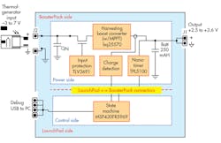
For evaluation and debug purposes, the design is packaged on a TI BoosterPack plug-in module for easy connection to the MSP430FR5969 LaunchPad Development Kit (Fig. 3). The MSP430FR5969 is a low-power 16-bit RISC microcontroller with 64 kB of embedded FRAM (ferroelectric random access memory). FRAM is a non-volatile technology that combines low power consumption with high endurance and high-speed write capability.
Although this discussion concentrates on thermal energy harvesting, the design is general-purpose in nature and is suitable for many applications, including solar chargers; wireless sensor networks; low-power wireless monitoring; bridge and structural health monitoring (SHM); portable and wearable devices; and more.
The TEG selected is a II-IV Marlow EverGen PowerStrap designed to harvest thermal energy from fluid-filled pipes or exhaust stacks (Fig. 4).
The bq25570 harvesting boost converter is designed to extract power efficiently from the TEG without collapsing the source. The bq25570 includes a Maximum Power Point tracking (MPPT) function to maximize the power transfer by matching the input impedance of the boost converter to the output impedance of the TEG, around 25 Ω for the Marlow PowerStrap.
The MPPT modulates the input impedance indirectly by regulating the charger's input voltage to a reference value derived from the energy harvester’s open-circuit reference voltage (VOC). The MPPT circuit obtains a new reference voltage by periodically disabling the charger and sampling VOC. The fraction of VOC used depends on the characteristics of the energy-harvesting device. For a TEG, it’s 50% of VOC; solar chargers require 70%-80%. Other values can be set with external resistors.
The bq25570 includes battery management to ensure that a rechargeable battery isn’t overcharged by the extracted power, or sees high or low voltages outside of safe limits. The device also incorporates a highly efficient, nano-power buck converter to provide regulated power for systems with stringent power requirements, such as wireless sensor networks (WSNs).
The TEG output voltage can swing below zero volts. In this case, a TLV3691 nano-power comparator detects the condition and turns off the load switch to protect the bq25570.
All of the components in the design are chosen for minimum power consumption. One of the issues with any energy-harvesting device is that sometimes no energy may be available for harvesting; for example, if there’s no temperature gradient across the TEG.
Under such conditions, the TEG is not charging the battery, which is the sole source of power to the system. If the battery becomes fully depleted, the system will cease to operate.
The TPL5100 Nano-Timer and Low-Power Operation
The design uses the TPL5100, another member of the nano-timer family, as a key part of a multi-level strategy to conserve the use of power.
In normal mode, the TEG charges the battery. All functions are enabled—the system is gathering application data and transmitting the results over the wireless link.
If the battery isn’t charging, the system transitions to an intermediate sleep state. The system still performs measurements and wireless communication is enabled, but the bq25570 is disabled to reduce the drain on the battery.
Once the battery voltage drops below the UVLO threshold, the system enters into a deep-sleep state. In deep sleep, no measurement or communication takes place. Power is shut off to all devices except the MPS430 and the TPL5100. The MPS430 is in its lowest-power mode and woken up by the TPL5100 every 1024 seconds (17 minutes), so that it can enable the bq25570 long enough to check whether the battery is charging.
If the battery is charging, the system will transition back to normal mode. If not, the system returns to deep sleep until the next TPL5100 wakeup. In deep-sleep mode, total power consumption is reduced to 130 nA—50 nA from the TPL5100 and 80 nA from the MPS430. In full operating mode, power consumption is typically 488 nA, with a maximum value of 900 nA.
Conclusion
Low-power operation is critical for battery-powered IoT applications. Although many such applications spend most of their time in low-power sleep mode, much can still be done to reduce current consumption even further, regardless of whether the battery is rechargeable or non-rechargeable. For rechargeable applications, an energy-harvesting design may supply sufficient energy for an indefinite operating life. In both applications, though, a nano-timer can manage the wakeup sequence with the lowest possible current draw.
About the Author
Paul Pickering
Paul Pickering has over 35 years of engineering and marketing experience, including stints in automotive electronics, precision analog, power semiconductors, flight simulation and robotics. Originally from the North-East of England, he has lived and worked in Europe, the US, and Japan. He has a B.Sc. (Hons) in Physics & Electronics from Royal Holloway College, University of London, and has done graduate work at Tulsa University. In his spare time, he plays and teaches the guitar in the Phoenix, Ariz. area
