This file type includes high-resolution graphics and schematics when applicable.
When devices are being designed to operate at low voltage, it’s often necessary to take into account the voltage drop across any diodes in the circuit. A challenging part of the design process is that the voltage drop across a diode depends on current flowing through it, which in its turn depends on the voltages in the circuit, including the voltage drop across this diode. It then becomes necessary to find the diode's voltage drop in a few iterations, and that can be cumbersome.
Also, the classical analysis of processes in a diode provides formulas that describe the current transfer through a diode, but the resulting diode characteristics, when plotted using the formulas, are different from those provided by diode manufacturers. This happens primarily because the classical physics formulas don’t consider resistance of bonding wires inside the diode, leads resistance, and other real-world factors.
The analysis here fills the gap between the physics theory and practical data, enabling designers to use analytical expressions that allow for an accurate analysis of circuits using silicon diodes. Equation 1 is a modification of a known Shockley formula (Equation 2) describing current flowing through a diode in dependence of the voltage across this diode within some temperature range.
where:
• Tj is the junction temperature of the diode, K
• Tj0 is the normal junction temperature, K
• θSi = 7K, the thermal coefficient for silicon, K
• q is the elementary charge, C
• k is Boltzmann's constant, m2·kg·s-2·K-1
• n is the imperfectness coefficient
• Is0 is the diode saturation current, A
• VD is the voltage drop across the diode
• ID is the diode current that creates VD
The formulas above don’t take into account the presence of the mentioned earlier resistances. These also affect the voltage drop across the diode, because we actually measure the voltage drop across the die itself plus the voltage drop across the bonding wires and other resistances. As a result, Equation 2 may be written as:
where rc is the resistance of bonding wires and silicon.
Equations 2 and 3 both have a factor:
which describes the saturation-current behavior while the ambient or die temperature changes. This model has a constant value Is0 and a power index that describes the saturation current’s dependence on ambient temperature. It’s conventional to use Is0 = 10-12 A to 10-14 A for silicon diodes, but best results may be obtained if its value is derived from a real diode characteristic.
From Equation 1, obtain the value for the saturation current Is0:
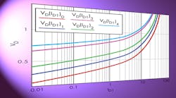
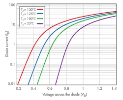
Its value may be obtained from a real diode characteristic by substituting the ID0 and VD0 values from a datasheet (Fig. 1) for Tj = 25â°C. Using Equation 4 in Equation 3 and solving with respect to ID, we can get:
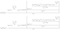
Equation 5 has a Lambert function, LambertW, whose solution is obtained by creating a special algorithm (and is beyond the scope of this paper).
The following example verifies the analysis:
Plot a diode characteristic at:
• Tj0 = 298 K
• θSi = 7 K
• k = 1.381·10-23 m2·kg·s-2·K-1 (Boltzmann's constant)
• q = 1.602 · 10-19 C (elementary charge)
and for ambient temperatures of 298 K, 373 K, 398 K, and 423 K (corresponding to 25â°C, 100â°C, 125â°C, and 150â°C), with n = 1.2 and rc = 0.02 Ω.
Using Equation 4 and the diode characteristic, find Is0 at normal temperature:
ID = 1.05 A at VD = 0.8 V
So Is0 = 1.128 · 10-12 A.
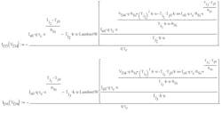
As the value of the LambertW function should be a scalar, we have to create four similar functions for the diode current versus the diode voltage:
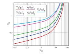
Use this in Equation 5 and create the graph (Fig. 2). Note that there’s close agreement between the results of the analytical model and the vendor datasheet values.
Gregory Mirsky holds an MS from the St. Petersburg Baltic Technical University, Russia, and a PhD from the Moscow State Pedagogical University. He has obtained multiple patents in USA and abroad, and has authored articles for a number of scientific and technical magazines.
