Enhance Thermal Performance Through Design And Optimization

When electrons flow through a resistive material, heat is generated. It’s not uncommon for high-power IC chips to dissipate greater than 50 to 100 W. A few years back, projections showed that chips would commonly reach 400 W or more. This increase in IC power levels has taken a back seat as energy conservation efforts have accelerated, as desktop computing has given way to battery-powered systems, and as cell phones and tablets strive for ever longer battery life.
As a result, power consumption growth rates have slowed and even reversed in some instances. At the same time, packages are shrinking to meet the needs of portable and space-constrained systems. Power densities can still be high, greater than 10 W/cm2, even though total power is reduced. If heat isn’t conducted from the die, overheating occurs with concomitant electrical failures.
Thermally under-designed systems often work when they’re first turned on. But as they heat and reach a critical temperature, they lock up. After being turned off and allowed to cool down, they work again. This behavioral “fingerprint” points to potential thermal under-design. Blogs covering various laptops, power supplies, and smart phones used to be rife with end users complaining about products overheating. Two trends are resolving these issues: self-sensing electronics that throttle device performance and power consumption when they begin to overheat and expertise in the art of system design to optimize thermal performance.
The Structure’s Role
The die structure itself is critical to thermal performance. Lumping power dissipative circuit elements in one location creates hotspots that can be difficult to cool. The thermally conductive silicon can help offset this problem. For example, thicker die are more effective at conducting heat away from power dense areas, resulting in improved hotspot cooling. Thinning the die, on the other hand, increases the spreading thermal resistance. Metallization on the die can help conduct heat from these hot spots, depending on their geometry and the metal layout, reducing temperatures. Alternately, the types and thicknesses of dielectrics on the die can impede thermal conduction, causing the die to heat.
Every structure that contacts the die becomes a thermally conductive path for the die’s heat. Everything touching the die is a heatsink. Within the package, die attach materials conduct heat from the die into lead-frame die pads or into copper planes in a substrate. Mold compounds conduct heat from the surfaces of the die and die pad to lead fingers or to the package surface (Fig. 1). As shown, wire bonds and substrate traces can conduct heat to package balls that conduct the heat into the printed-circuit board (PCB), which acts like a heatsink for the package.
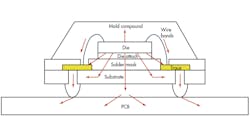
1. An over-molded, wire-bonded IC package attached to a system-level PCB can take advantage of common thermal conduction paths (shown in red) for cooling.
The heat-spreading efficiency of a package primarily depends on the layout of the metal structures within it. Why? Copper’s thermal conductivity is 386 W/m-°C at room temperature. Solder conductivities range from 30 to 60 W/m-°C depending on the alloy implemented. Compare this to insulating polymer conductivities of 0.1 to 2 W/m-°C, depending on the filler material. The polymers are two or more orders of magnitude less thermally conductive than the copper. Metal in the package and the system board and chassis will conduct most of the heat.
The design of the metal must be carefully controlled for thermal management. To keep the chips cool, high thermally conductive metal paths must be implemented to spread the heat for improved convection and radiation into the system environment. Each package type will have its own set of thermal paths that require optimization.
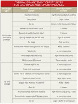
Designers should use the common thermal paths for wire-bonded lead-frame packages and for flip-chip substrate packages when they are available, but they often aren’t (see the table). For example, pins are infrequently connected to the pad of a lead-frame package due to process complexity, costs, and sometimes reliability risks. It’s the responsibility of the package designer to understand the special configuration of each package and assess the important thermal paths that require optimization.
A system viewpoint is critical for package thermal enhancement. For example, if heatsinking is expected, thermal conduction from the die to the heatsink mounting surface must be optimized. Efforts are required to make this path as thermally conductive as possible. If the PCB is to be used as the heatsink, heat conduction paths from the die through thermal vias in the package (or exposed thermal pads) into thermal spreading features in the PCB are required (Fig. 2).
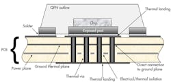
2. This four-layer PCB cross section shows a package with an exposed pad soldered to a thermal landing that is connected to the PCB ground plane through thermal vias. The vias are isolated from the power plane for electrical reasons. In this figure, the ground plane would become the thermal spreading plane assuming it was continuous over a large area
The PCB must have sufficient spreading area on each device to convect and radiate the required heat load (Fig. 3).
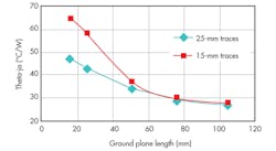
3. The area of the heat-spreading planes that connect to the IC package determines a PCB’s cooling efficiency. The effective qja of a 12- by 12-mm chip-scale package with 49 thermal balls as a function of the (x,y) length of a plane under the package is plotted up to 104 by 104 mm. Two trace lengths were assumed, showing different amounts of coupling of heat from the traces into the plane.
Also, the designer must understand whether the board will be air cooled by fans, by a vented enclosure, or even by the orientation of the board with respect to gravity. Unintended consequences should be anticipated during risk analyses. For example, if the system is cooled passively through slots, what happens when the end user drapes a coat over it or when dust accumulation fowls the slots? Are there margins in the design to guarantee good operation under adverse conditions?
Best Practices
To be successful, good thermal engineers will incorporate six steps into their design practices:
• Determine the power that will be dissipated under all use conditions.
• Ensure all design inputs such as thermal properties are accurate.
• Identify the range of thermal enhancements that fit the application space and system cost targets.
• Iterate through modeling to find multiple design solutions.
• Share the solutions with the co-design team early and accept feedback.
• Validate the modeling predictions to improve the process for future designs.
Thermal design engineers must also avoid common pitfalls. For instance, they must not focus on optimizing one thermal path at the expense of others. As a laundry list, improving thermal conduction from a chip to the PCB won’t have much impact if the PCB is not adequately designed to spread the heat or if too much heat is already being dumped into the PCB.
Improving airflow may not fix a system that doesn’t have sufficient heatsinking at even the most aggressive airflow velocities. Putting an efficient heatsink in a region of the system without airflow won’t result in much thermal enhancement. If a system cable blocks the airflow, the heatsink will become ineffective. Smearing traces in a system PCB to make the modeling task easier can hide isolation cuts in metal planes that block the conduction of heat. All environmental conditions must be considered. For example, sunlight during outdoor operation can dump more power into the system than the electronics are generating.
Software tools are a must for thermal enhancement and optimization. Thermal engineers should be intimately familiar with their tool of choice, knowing its strengths and weaknesses. Factors such as convergence, mesh sensitivity, and mesh simplification must be addressed to ensure accuracy.
The largest source of error in a system thermal analysis is usually the estimate of the power that will be dissipated by the system. This is especially true of programmable systems where power dissipation is a function of the software and features exercised. For example, video editing on a tablet uses different instruction sets than game playing or book reading. Web page rendering on one piece of software can take much more power than Web page rendering on another. Common practices are to design the system for most normal usage levels while enabling thermal overrides to throttle the system when high-power operations push toward thermal overheating.
Even with reduced device power dissipation, increasing complexity and miniaturization is driving thermal management requirements. Design discipline is essential to eliminate overheating in systems and to provide optimal thermal solutions at the lowest cost. Complex systems must operate reliably over their intended lifetimes. Thermal issues can be overcome with upfront knowledge of thermal enhancement options, die-through-system co-design, and thermal risk analysis.
Darvin Edwards, TI Fellow, manages the SC Packaging modeling team at Texas Instruments. His team is responsible for electrical, thermal, and thermomechanical analysis of new products and package developments. He received his BS in physics from Arizona State University and holds 20 patents. He also has authored or co-authored over 45 papers, articles, and book chapters and has lectured on thermal challenges, modeling, reliability, electrostatic discharge (ESD), and 3D packaging.
About the Author
Darvin Edwards
Darvin Edwards, TI Fellow, manages the SC Packaging modeling team at Texas Instruments. His team is responsible for electrical, thermal, and thermomechanical analysis of new products and package developments. He received his BS in physics from Arizona State University and holds 20 patents. He also has authored or co-authored over 45 papers, articles, and book chapters and has lectured on thermal challenges, modeling, reliability, electrostatic discharge (ESD), and 3D packaging
Comment About the Article
To join the conversation, and become an exclusive member of Electronic Design, create an account today!

Leaders relevant to this article: