Download this article in PDF format.
Silicon MOSFET power transistors have been a mainstay of power-supply design for years. And while they’re still widely used, gallium-nitride (GaN) transistors are gradually replacing MOSFETs in some new designs. Recent developments in GaN technology, plus the availability of improved GaN devices and driver circuitry, have more designers looking at the GaN option. GaN offers clear benefits over conventional MOSFETs such as greater switching speeds and higher efficiency.
GaN Devices
GaN power transistors have been around for several years now. Early devices were made on expensive substrates, such as sapphire or silicon carbide (SiC). The primary application was RF power amplifiers for high frequencies. Thanks to their high electron mobility and high voltage tolerance, these devices can generate hundreds of watts of power at frequencies well into the gigahertz range.
Such transistors are called high electron mobility transistors (HEMTs) or pseudomorphic HEMT (pHEMT). HEMTs are a form of metal-semiconductor junction FET using different materials for the gate and channel. These are “depletion-mode” types of FETs, meaning they’re naturally “on,” unlike the enhancement-mode naturally “off” MOSFETs. HEMT FETs require critical bias networks for proper operation.
1. This power-system configuration is commonly employed in data centers.
A more recent development is the enhancement-mode GaN FET, or eGaN. It’s of the insulated-gate variety. Like all GaN devices, they offer the benefits of higher-speed switching, higher voltage operation, and improved heat dissipation. Though enhancement-mode GaN devices are still more expensive than silicon MOSFETs, they’re more suitable for power-supply designs and offer a design path to greatly improved performance and efficiency.
The Case for High-Voltage Designs
Switch-mode power-supply (SMPS) designs are the answer to improving efficiency and conserving energy. Most new designs apply SMPS technology, including regulators, dc-dc converters, point-of-load (POL) converters, and inverters. However, even SMPS designs can be improved.The Case for High-Voltage Designs
It has been shown that efficiency declines with each power-conversion stage in the design. Converting high line voltages to low dc supplies for processors and FPGAs typically requires multiple stages of dc-dc conversion and regulation. Reducing the number of conversions is possible if high-voltage devices are available to make the conversion. GaN devices offer that potential.
An example is a data-center power system. Data centers contain many high-power servers that require low voltages at high currents. The power is expensive, but so is the cooling that’s required. Any savings in the power-conversion path is worthwhile. Figure 1 shows a typical supply with 120- or 240-V ac input.
A power-factor-correction (PFC) stage is required by the electric utility. This is usually a boost converter with a dc output of 380 V. It’s passed to an inductor-inductor-capacitor (LLC) stage that provides a dc output of 36 to 60 V. This is further stepped down by a dc-dc converter, then on to POL converters that provide 1 to 1.8 V dc for the processor, memory, and FPGAs. Each stage takes its toll on efficiency.
2. Here, the power system was improved by implementing different circuit topologies and fewer stages to improve efficiency.
Figure 2 shows the solution to this problem. The PFC stage topology is changed with GaN devces that can operate at higher voltages and at higher speeds. The higher switching frequency means that any magnetic devices can be much smaller and more efficient. The LLC stage, also using GaN, downconverts to a 36- to 60-V output utilizing switching frequencies above 1 MHz. A typical output is 48 V to the POL converters, which are exploiting GaN as well. The overall design is not only smaller, but also more efficient.
Another application involves solar inverters. The solar panel usually drives a dc-dc boost converter. That converter, in turn, operates the dc-ac inverter that provides the 120/240-V ac 60 Hz that ties to the load and the grid. Some systems may include battery storage. Using GaN in both stages and a switching frequency well in excess of 100 kHz greatly improves efficiency over current designs.
In addition to dc-dc converters, POL converters, and inverters, other GaN applications include motor drives and Class D high-power audio amplifiers.
A Breakthrough Product
Designing with the eGaN FET devices can be challenging mainly due to the tricky gate-drive circuits. In addition to providing the right gate-drive voltage to the GaN power FETs, the circuitry must also provide protection for overvoltage drive or undervoltage conditions.
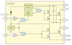
3. The LMG5200 hybrid multichip module, which features two GaN FETs, helps protect against overvoltage and undervoltage.
One device that solves the problem is Texas Instruments’ LMG5200. This hybrid multichip module (MCM) contains two 80-V, 10-A GaN FETs in a half-bridge configuration with integral driver. Figure 3 shows the functional block diagram. Note the undervoltage-lockout (UVLO) protection that prevents the FETs from partially turning on if the input supply voltage falls too low. A clamp also prevents the high-side gate drive from exceeding the FETs’ maximum gate voltage.
Features of the LMG5200 include 15-mΩ on-resistance GaN FETs, 80-V continuous or 100-V pulsed rating, gate driver capable of up to 10-MHz switching, TTL inputs, 10-ns minimum PWM width, and 29.5-ns propagation delay. The device comes in a 6- × 8- × 2-mm, 9-lead QFN package. When used with TI’s TPS53632G controller, the LMG5200 enables direct conversion from 48 V to 0.5-1.8 V in POLs. An evaluation module is available.
Also, check out this video to learn more about how GaN can revolutionize power-conversion designs.


