Identifying EOS And ESD Failures In Semiconductor Devices
ICs subjected to electrostatic discharge (ESD) stress have distinct failure signatures. High currents can melt different regions of the semiconductor structure (ESD-HBM, or human body model), while high electric fields can rupture dielectrics (ESD-CDM, or charge device model).
The most common ESD-induced failure mode, open, shorts, leakage or resistive shorts at input/output pins, can be observed on ESD induced units by curve tracing, bench or automated test equipment (ATE) tests. Other failure modes may have high shutdown current (IDDS), supply current (IDD), and open pins such as no output. Internal circuitry damage requires advanced failure analysis techniques.
This file type includes high resolution graphics and schematics when applicable.
EOS and ESD can destroy a semiconductor device in many ways. Most EOS and ESD subjected failures occur mainly due to thermal damage or burnt metallization, oxide or dielectric breakdown, contact damage, or junction damage.
Thermal Damage
Field failures due to thermal damage can occur when the excessive heat generated during an EOS-ESD event melts the metal interconnects of conductors or resistors. The excessive heat generated during an EOS-ESD event can melt the metal interconnects of conductors or resistors. The metal line that acts as a fuse may become open after melting. Metal melting commonly is observed due to an EOS, ESD-HBM event. In thick conductor films, though, partial melting of the metal may impact the functionality of the device. If the metal line has resistance R and IESD is the current flowing, then the power generated will be:
P = I2ESD*R
When temperature due to localized heat is raised to the melting point of the metal line, melting will occur. The device might not show pin-to-pin I/V curve abnormalities, such as short or opens. But after decaping, scanning electron microscopy (SEM) reveals burnt metallization (Fig. 1).
Oxide Or Dielectric Breakdown
Oxide breakdown can be categorized as a soft or hard breakdown. Soft breakdown refers to a high resistive current path across the dielectric. Hard breakdown refers to a highly conductive path across the dielectric layer.
In a soft oxide breakdown, the device may functionally good and the performance of the transistor will not be changed significantly. The leakage can be observed to be a little higher than good units and may fall within datasheet limits. In a hard oxide breakdown, the device is not operative, a current path is created from the gate to the channel, and the transistor is destroyed.
Gate oxide damage is the most common and prone to ESD events. Gate oxide breakdown depends upon the thickness of oxide, biasing voltage, breakdown voltage of oxide material, uniformity, and roughness of oxide film. If the oxide film has sharp edges, the induced electric field will be highly concentrated to those edges and highly prone to breakdown.
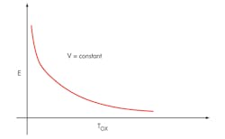
Consider the oxide layer to have a thickness of 100 Å with applied voltage across the oxide layer of 3.3 V. The average electric field across the oxide layer then can be calculated from E = V/TOX:
E = 3.3 V/(100 x 10–8 cm) = 3.3 x 10⁶ V/cm
Silicon dioxide (SiO2), a dielectric material, has a breakdown electric field of 11 x 106 V/cm. If the oxide thickness is reduced to 50 Å, then:
E = 6.6 x 10⁶ V/cm
There will be an increase in the electric field across the dielectric as it approaches breakdown. If V is kept constant, i.e. E/TOX = constant, the electric field versus oxide thickness curve can be represented by Figure 2.
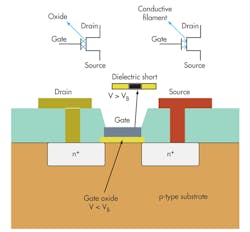
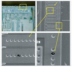
Oxide breakdown could occur as a voltage across the oxide layer exceeds the breakdown voltage (V > VB) of the oxide (dielectric). As a result, the gate oxide breaks down and a less resistive path is formed across the oxide layer. Because current is flowing into a less resistive path (damaged oxide or dielectric), localized heating of the dielectric occurs. Due to large localized heat, the conductive site melts down, forming a filament that shorts the metal layers across the dielectric (Fig. 3). Oxide breakdown is known as the main breakdown mechanism of the CDM.
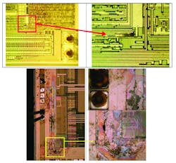
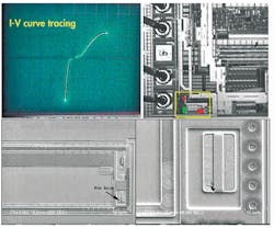
An ESD-CDM event also can cause an oxide rupture (Fig. 4). In this failed part, no output was observed on the bench test. In electrical isolation, high leakage at the reference input pin of the oscillator circuit was measured. Hotspots also were detected along the capacitor of the reference input pin in the oscillator block.
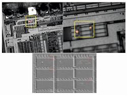
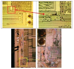
Figure 5 shows the ESD damage of a crystal oscillator device where no output was observed. The bench test (I-V curve tracing) showed leakage of 4.3 mA at the output enable (OE) pin. The fault site was isolated using the Hamamatsu emission/OBIRCH microscopy to localize the defect. The hot spots were detected along the input circuitry of the failing pin. Subsequent physical analysis using plasma/chemical etching revealed a pinhole at a hotspot area identified by the emission microcopy.
Contact Spike Or Junction Damage
A contact spike or junction damage refers to the destruction of a p-n junction due to joule-heating caused by an ESD event. When silicon gets heated, covalent bonds are broken and charge carriers are generated. Thus, silicon resistivity and thermal conductivity decrease with an increase in temperature.
ESD pulses behave like current sources. When a sudden ESD pulse is subjected to silicon, it heats unevenly. The localized area gets heated adiabatically when a large current flow raises the junction temperature and exceeds the melting point of silicon as a result junction melts (Fig. 6).
The energy dissipation due to ESD causing a contact spike or junction damage can be calculated. For an adiabatic process, the energy created by the ESD event is equal to the energy absorbed by the junction:
Q1 = Q2
where:
Equating Q1 = Q2:

where:
Csp = specific heat capacity
ρ = density
T0 = initial temperature
If T ≥ Tm (melting point), then the junction melting will take place.
The Wunsch & Bell model that uses a thermal diffusion equation as given below is most generally used as the model to describe this junction breakdown. In the model, the junction breakdown phenomenon is determined from the pulse width and power density that are applied to the device:

where:
P = power to failure in watts
A = area in cm2
CP = heat capacity in J/gcm-K
ρ = density in g/cm3
κ = thermal conductivity in W/cm-K
t = width of a square pulse
Tm = melting temperature of the junction
T0 = initial temperature
These expressions show the relation between temperature, ESD pulse voltage, power to failure, and the melting point of the material.
References
1. Electrostatic Discharge: Understand, Simulate, and Fix ESD Problems, M. Mardiguian, Wiley
2. “Charging by Walking,” Niels Jonassen, Compliance Engineering, March/April 2001, www.incompliancemag.com/index.php?option=com_content&view=article&id=2016:charging-by-walking&catid=62:mr-static&Itemid=201
3. “Electro-static Discharge (ESD) Tutorial,” Ata Khan, Cypress Semiconductor, www.cypress.com/?docID=35736
4. “ESD Protection Circuits for Advanced CMOS Technologies,” Jung-Hoon Chun, 2006, www-tcad.stanford.edu/tcad/pubs/theses/chun.pdf
5. “Electrostatic Discharge Protection,” Fei Yuan, Ryerson University, 2012, www.ee.ryerson.ca/~fyuan/esd.pdf
6. “Investigation of Device Damage Due to Electrical Testing,” Rosa Croughwell and John McNeill, Worcester Polytechnic Institute, www.teradyne.com/atd/resource/docs/testStation/tpWPI.pdf
7. “Electrostatic Discharge in Semiconductor Devices: An Overview,” James E. Vinson and Juin J. Liou, 1997, www.lorentzcenter.nl/lc/web/2010/424/PROBLEMS/NXP/ESDreviewvinson98.pdf
8. “Electrostatic Discharge Protection Circuit for High-Speed Mixed-Signal Circuits,”
Hossein Sarbishaei, 2007, https://ece.uwaterloo.ca/~cdr/pubs/Hossein_PhD_thesis.pdf
9. “Fundamentals of Electrostatic Discharge, Part One—An Introduction to ESD,” ESD Association, 2013, www.esda.org/documents/FundamentalsPart1.pdf
10. ADI Reliability Handbook, 2000, www.analog.com/static/imported.../eos_esd_chapter_091400b_103.pdf
11. “Breakdown voltage of ultrathin dielectric film subject to electrostatic discharge stress,” Hao Jin et. al, Journal of Applied Physics 110, 054516 (2011)
12. “Electrostatic Discharge and Electrical Overstress Failures of Non-Silicon Devices,” Yu-Chul Hwang, 2004, http://drum.lib.umd.edu/bitstream/1903/2198/1/umi-umd-2198.pdf
13. “Electrical Overstress,” www.cypress.com/?docID=20619
Sanjay Agarwal is a senior product engineer working in timing solutions at Cypress Semiconductor, Bangalore. He holds a master of technology degree from the Indian Institute of Technology Kanpur, specializing in electronic materials, device fabrication, and characterization. He has authored numerous technical articles for semiconductor electronics publications.
About the Author
Sanjay Agarwal
Sr. Product Engineer
Mr. Sanjay Agarwal is working as Sr. Product Engineer in Timing Solution, Cypress Semiconductor, Bangalore. Mr. Sanjay Agarwal holds a Master of Technology degree from Indian Institute of Technology Kanpur specialized in Electronic Materials, device fabrication and characterization. He has authored numerous technical articles in semiconductor electronics publications.
Comment About the Article
To join the conversation, and become an exclusive member of Electronic Design, create an account today!

Leaders relevant to this article: