Limit Inrush Current in AC-DC Power Supplies and Rectifiers
Rectifiers and ac-dc power supplies employ large bulk capacitors. During power-up, these capacitors require a large amount of current to charge up, resulting in a large inrush current. This inrush current creates limitations in the operation of power devices and interference of those devices with the power line and circuit breakers. It also affects the reliability of the power system due to overstress caused by instantaneous but huge surge in initial current at power up. Known solutions to limit inrush current1,2 require resistors or conventional NTC thermistors, which contribute significant power loss and decrease the efficiency.
This file type includes high resolution graphics and schematics when applicable.
To overcome many of the existing technology’s disadvantages in limiting inrush current in high-power ac-dc power supplies and rectifiers, IXYS developed the Digital Inrush Current Controller. It combines the company’s digital power-control technology with Zilog’s 8-bit Z8F3281 MCU to limit capacitor pre-charge current to a predetermined value at each half sine-wave cycle. Capacitor charge is spread over a number of cycles until the capacitor is charged proportionally to a peak value of ac voltage source.
The controller features programmable overload protection and a “Power Good” status signal. It’s not sensitive to power outage, brownout, and ambient temperature variations. It can operate over an input-voltage range of 80 to 240 V ac, and load current up to 3 A. The entire operation’s process and essential values are fully programmable—the controller may be programmed to 50 Hz, 60 Hz, or any other line input frequency operation.
Time-Dependent Pulse Train
Figure 1 illustrates a conceptual circuit schematic that’s designed to deliver charge to the bulk capacitor in equal increments. The capacitor is charged according to a time-dependent pulse train driving transistor SW1. The pulses are designed in a way to provide substantially equal voltage increments to the capacitor to keep peak charging current at about the same value for each cycle. The number of cycles depends on the capacitor value, and selection of the charge current correlates to the desired ripple’s amplitude at the output. Charge current is a function of the number of pulses and the timing position with respect to the rectified sine wave.

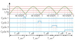
Figure 2 shows an example of generating the pulse train for SW1. If we can consider N cycles for inrush control, then we can split the normalized amplitude of half-rectified sine wave to N segments with an increment of 1/N as shown. During cycle 1, SW1 is on (conducting) from the time stamp t1 to T, thus making the capacitor C charge to the voltage proportional to normalized value 1/N. The charging current doesn’t rise instantly because it’s a current in a serial LC resonant circuit that shapes the current waveform to the resonant one. The current rises until the capacitor’s voltage reaches input voltage.
Subsequently, current continues its resonant behavior because SW1 is still conducting. No further oscillation occurs because input voltage drops below voltage on the capacitor, and then SW1 is off (not conducting). The capacitor remains pre-charged to the voltage proportional to 1/N. In Cycle 2, capacitor C is pre-charged by another voltage increment 1/N in the process similar to cycle 1. Capacitor C is charged N cycles to the voltage value proportional to the input-line voltage.
Principle of Operation
Another variable to control inrush current is LC time constant. Capacitor C value depends on desired ripple value. After selecting the capacitor C value, the designer can decrease peak inrush current by increasing inductance L. If there are physical limits to the L value, the number of cycles N should be used to set the required peak current. Turn-on time for switch SW1 should be defined for each active cycle.
For cycle 1 in Figure 2, the delay from the zero crossing point (point 0 in Figure 2) to the beginning of turning on SW1 (t1) is denoted as T_off. The time between t1 and T, an active time to keep SW1 on, is denoted as T_on, and the period or cycle duration is denoted as T.
Active time T_on for each occurrence “i” is defined as geometrical transform:

where i - 1...N.
The period T is measured by the MCU at initialization. Values of T_on are determined by Equation 1 and stored in memory. Values of T_off are derived by firmware according to following expression:
T_off = T – T_on (2)
Figure 3 illustrates a conceptual algorithm that’s executed in MCU Z8F3281 for the first four cycles of inrush control. The timing counter corresponds to time at any given moment of a discrete time base provided by the internal clock. The counter first counts from zero crossing to the T_off value. When the counter reaches the T_off value, it initiates a T_on pulse (black line on Figure 3) that continues until the counter reaches the T_on value, finalizing one charging cycle. The rectified power-line voltage (blue line) is shown for reference.
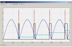
Figure 4 illustrates the timing position and amplitude of the capacitor’s current (red curve) with respect to T_on pulses. It should be noted that the Inrush Controller generates a single current pulse during each cycle. The capacitor’s charge is complete when input voltage drops below capacitor voltage. The input power line is isolated from the rest of the circuitry by the diode bridge circuit, and the inductor discharges into the capacitor. Then SW1 is turned off (not conducting) up to the end of the cycle. The algorithm is based on reactive power transfer, hence, losses are limited mostly to those on strain resistance.

Figure 4 shows that the capacitor’s pre-charge is finalized at time-stamp 0.066 ms. After that, the Power Good (PG) signal is generated and load is activated. The capacitor’s current shows up as negative beginning at time-stamp 0.066 ms, because current is sourced from the capacitor when the load is activated. The Power Good signal can be delayed with respect to end of pre-charge of capacitor C so that the load can stabilize before executing other functions. The overload threshold is programmable, too, and is set to 3.5 A.
Overload Protection
Overload protection protects a device from damage in case of overload or continuous overload. If a comparator detects overload, then the MCU disconnects the capacitor from the load by turning off SW1. Also, the PG signal is set to logic low to disable the load if possible. Overload protection can be programmed for two modes of operation: immediately shut down the device and wait for user interference; or allow a device to restart a predetermined number of times.
After initial pre-charging and connecting the load, the MCU may be reconfigured for other power-management tasks. For example, it can perform power-factor-correction (PFC) control and keep track records on device performance, overload conditions, power outages, power brownouts, etc. With the collected information, the MCU is able to inform the user on the state of the device’s reliability and supply system performance data.
Digital Inrush Controller
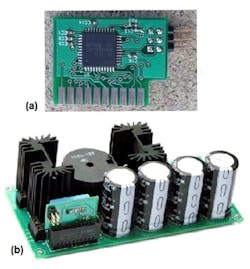
IXYS’s Digital Inrush Controller consists of an MCU module and main power board (Fig. 5). Figure 6 shows detailed circuit schematics. The MCU module, implemented as an add-on device, has a connector for MCU programming. The MCU should be programmed before powering the entire system. An auxiliary power supply powers the module, providing +3.3 V for the MCU and 12 V for the gate driver applied to connector J4 on the main power board.
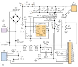

The main power board is a two-layer printed-circuit board (PCB) with a diode bridge and MOSFET Q1 (SW1) mounted on small heat sinks. Power dissipated on these heat sinks is less than 5 W at 375-W output power. This board may be powered from a 50- or 60-Hz ac source.
Inrush-Controller Testing
The controller’s performance has been verified by several bench tests, such as that revealed in the scope snapshot in Figure 7. Testing confirmed that the inrush current is limited to a predefined value and limiter performance is quite close to simulation results. The amplitude of the inrush current is limited to the value of the input current at maximum load by selecting the number of inrush current pulses equaling 16 and the inductor value to 100 µH. It minimizes the negative impact on the ac line, and limits electromagnetic interference (EMI). During the test, the ac input line is connected through an isolation transformer as a precaution. The Power Good signal connecting load is generated at the rectified voltage zero crossing one cycle after the output capacitor is completely charged (see the red line in Figure 7).

Figure 7 depicts SW1 gate drive pulse T_on time (yellow line) and rectified voltage (green line) at the input of the device. Rectified voltage slightly drops after the load is connected due to the limited output power of the isolation transformer used during the test. The blue line depicts line current and the red line depicts the load voltage. The system is verified to provide 2.5-A output current at full load at normal operation. Inrush current is limited to 10 A.
Measured efficiency of the inrush control path is 99.5%. The device can work over a wide input voltage range of 80 to 240 V. Tested power-line frequency range was 50 Hz and 60 Hz; dedicated control pulse train was developed for each power-line frequency. In case of higher power-line voltage, a longer control pulse train is needed to keep the same amplitude of the inrush current. For instance, if the ac line voltage is 220 V, it requires a double pre-charging time to have the same peak inrush current when at 110 V.
Overload protection is based on continuous monitoring of the dynamic current from the bulk capacitor, In case of an overload condition, the current drawn from the capacitor instantly increases and the comparator inside the MCU initiates the system overload mode. Overload current threshold, number of overload instances, and the period between overload events are programmable.
The system response was verified successfully by testing an overload condition. The load was increased to draw an output current of 3.5 A, which triggered an overload protection. The system was also tested with continuous overload, resulting in multiple attempts to restart the system with immediate interruption. Power Good status is not present in overload conditions. Overall, this overload protection isn’t sensitive to power interruptions, brownout, and temperature variations.
Conclusion
IXYS’s Digital Inrush Controller offers flexibility with its unique control algorithm that aids in creating an efficient power system. Testing results show that it achieves a high level of efficiency, increased stability, and reliable performance over a wide load range. Thanks to an innovative current-measurement algorithm, it allows for common input and load grounds. Users can optimize the device for a wide range of input voltages and frequencies. In addition, the design provides instant overcurrent protection, followed by an intervention by the MCU for corrective actions.
This file type includes high resolution graphics and schematics when applicable.
Leonid Neyman, Senior Application Manager at IXYS, holds a Master’s degree in electromechanical engineering from Saint Petersburg State University of Aerospace Instrumentation, Russia, and Ph.D. degree in electronics engineering from Saint Petersburg State Electrotechnical University, Russia. His main engineering field is mixed analog/digital design, and is the author of 28 patents.
Anatoliy Tsyrganovich, Fellow Systems Architect at Zilog (an IXYS division), holds Master’s and PhD degrees in digital signal processing. Along with video and audio, his engineering field of expertise is in developing extreme efficiency of power converters via digital-control techniques. He is author of over 30 patents.
Abdus Sattar, Director of Engineering for power devices and applications at IXYS, holds an M.S in engineering (electrical) from South Dakota State University, Brookings, and a PhD (electrical) from Santa Clara University, Calif. He is the author of several publications and patents in electron device physics.
References
1. Randhir Singh Malik, William Hemena, Circuit for limiting inrush current to a power source, US6445165 B1, Sep 3, 2002.
2. Michael Allen, Understanding power supplies and inrush current, Electronic Products, March 2006, pp. 64, 65.
About the Author
Comment About the Article
To join the conversation, and become an exclusive member of Electronic Design, create an account today!

Leaders relevant to this article: