Modeling Op-Amp Output Impedance: A New Approach
When used with other blocks and modules, a new approach to modeling operational-amplifier output impedance behavior can provide a more realistic overall behavioral model. Simulating the behavior of a part or system prior to fabrication or building a system with behavioral models to optimize performance is an essential part of the design process. In addition, engineers can benefit from evaluating the part’s performance as a standalone device or in a system.
This file type includes high resolution graphics and schematics when applicable.
Model Evolution
The Boyle model was the first comprehensive and most famous op-amp model.1 It was introduced in the 1970s and still is being widely used today. While in many aspects the Boyle model is very primitive, it has proved itself to be useful in many different applications.
In the Boyle model, a resistor represents the output impedance, which cannot depict a frequency response. Other modeling methods introduced a filter of sorts to shape the output impedance frequency response. However, a new model for output impedance can reproduce the frequency behavior of output impedance with basic ideal components.
The simplest op amp comprises a few basic components: the input resistance, a gain element, and output resistance (Fig. 1a). The input resistance is between two input terminals and is connected to a voltage-control-voltage-source (VCVS). The gain of VCVS sets the op amp’s open loop gain. The output resistance is represented by a resistor connected in series from VCVS to the output node.
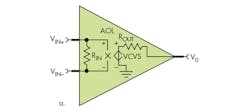
This model simply provides the coarse representation of dc gain and input and output impedance, which is barely adequate for most circuits or systems. If a pair resistor and capacitor is added as a low-pass filter to the gain stage, the op amp’s bandwidth can be introduced to model and shape its frequency response.
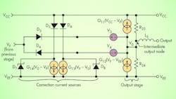
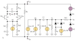
Boyle then introduced a more complete model capable of introducing a few more parameters such as current limit, slew rate, and output clamp (Fig. 1b). In 1990, Alexander & Bowers came up with a new model for op amps.2 It was based on Boyle’s original model with improvements that introduced new parameters (Fig. 2).
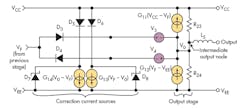
The input to every stage came from the previous stage while it was being referenced to an internal reference point (VREF), which was calculated based on the supply voltages:
VREF = (VDD – |VSS|)/2.
A New Approach
Up to this point, no models could provide a dynamic and robust production of output impedance. They were limited to either the dc representation of the output impedance or the frequency shaper used for output impedance, which could not adapt to a more complicated variation of output impedance.
Alternative approaches can provide more output impedance control. One model introduces multiple poles and zeros to output impedance. Much like the approach used in gain stage, capacitors, inductors, and resistors can be added to introduce the desired number of poles and zeros in the frequency response of output impedance.
Similarly, one can introduce a module with a series of low-pass and high-pass filters in a negative feedback to achieve the same result. These methods control how the impedance is shaped very well and can closely match the output impedance response to the behavior of the actual part. While these approaches are superior to those previously mentioned, introducing additional knobs to control or adjust the behavior is difficult.
One of the main goals during development of the output impedance block was modularity. The output impedance module must be easily adjustable and easily inserted into or removed from the main amplifier block. By creating a module that could be plugged in or removed, a wider variety of amplifiers and applications can be covered.
In amplifier macromodels, the gain and frequency shaping stages are placed prior to the output impedance. Given the location of the output impedance block, it should not attenuate or amplify the input signal. For example, it should exhibit unity gain from input to output. To tackle modularity, a two-port network approach is used as the starting point (Fig. 3).
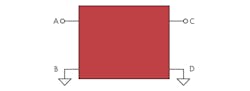
Based on these constraints and goals, the impedance module must satisfy two basic conditions. First, looking into the module from C, it should exhibit controllable impedance and frequency dependency. Second, the gain from A to C is unity. For this purpose we start from basic building blocks, continue with the impedance gyration concept, and conclude with implementation.
Frequency-Dependent Resistor
Generally, the amplifier’s open-loop output impedance can be modeled as a resistor with some frequency dependency:
Z(s) = R*(Z(s)/P(s)) (1)
The precise characteristics of impedance across the desired range of frequency depend on the amplifier’s output stage under test. The scope of this project was to create an impedance module that could be modeled with poles and zeros, created using either of two circuits (Fig. 4).
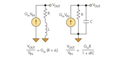
One thing to consider, though, is that a bare “zero stage” requires the use of an ideal inductor. An ideal inductor can generate infinite voltage when the current through it changes instantaneously, creating convergence issues in Spice. To avoid convergence issues caused by the non-causal zero stage, various circuit combinations can generate a pole/zero or zero/pole pairs, which are more desirable for implementation.
The OTA
Before delving deeper into the inner workings of the impedance block, it is important to understand the basic building block used to create the model: the operational transconductance amplifier, or OTA (Fig. 5).
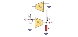
In an ideal OTA, the output current is a linear function of the differential input voltage, calculated as:
IOUT = (VIN+ – VIN–)gm (2)
where VIN+ and VIN− are the voltages at the non-inverting and inverting inputs and gm is the transconductance of the amplifier. OTAs are very useful building blocks and can be found in a wide variety of applications in circuit designs, from filters to the differential input pair of an op amp.
Assuming that the input impedance of the OTA is infinite, or that there are no current flows into the V+ or V– terminals, these expressions can be drawn:
IZ = gm1VIN (3)
VZ = IZZ (4)
Thus:
VZ = gm1ZVIN (5)
Now:
I2 = gm2VZ (6)
Substituting Equation 5 in Equation 6 yields:
I2 = gm1gm2ZVIN (7)
Since for an ideal OTA:
I2 = IIN (8)
Substituting Equation 6 in Equation 7 gives:
IIN = gm1gm2ZVIN (9)
Rearranging:

Looking closely at Equation 10, notice that the impedance Z has been “inverted” into an admittance multiplied by a scaling factor of 1/gm1gm2. The impedance inverter or gyrator can be used to invert a capacitive load and emulate a relatively large inductive load. This is very useful when passive inductors are not practical due to size or cost.
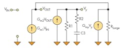
Cascaded Gyrators
Based on the principle explained earlier, gyrators can be cascaded to build what is known as the impedance multiplier (Fig. 6):
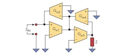


Similarly, let gM3 be in the form of:

Then Equation 11 becomes:

Letting gm1 = gm2 = gm3 = gm4, Equation 13 can be rewritten as:

As a result, a frequency-dependent resistor is achieved by using only OTAs and capacitors. Taking a closer look at Equation 12a, it becomes clear that if poles and zeros are considered, then it can be rewritten as:

Since an OTA is a voltage-controlled current source, feedback can be used to transform this conductance into a resistance, also known as the source absorption theorem—the same principle used in diode-connected transistors. By applying feedback, the whole circuit can be reduced to a voltage-controlled resistor circuit where:

The system in Figure 7 was used for final implementation due to its simplicity.

A pole/zero pair can be implemented as in Figure 8.
Unity Forward Transmission
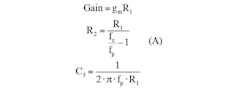
So how is the frequency-dependent resistor used in a circuit? Since our model represents a grounded resistor, it is convenient to drive this module with a current source. Given the input to the module is voltage, an OTA can be used to drive the ZOUT module. Therefore, the gain from input to output can be written as:

where gm1 is the gm of driver stage and gm2 is that of frequency-dependent resistor. To obtain unity gain at dc VOUT/VIN = 1:
gm1 = gm2 (18)
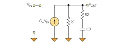
To illustrate the use of the output impedance module, assume the output impedance module needs to display a behavior as in Figure 9.
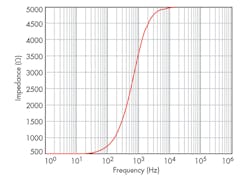
Reducing the behavior in Figure 9 to model parameters, the following assumptions can be made:
• The value of R = 500 Ω, thus gm2 = 2 ms
• There is a zero at F = 100 Hz
• There is a pole at F = 1 kHz
Moving to the driver stage:
gm1 = gm2 = 2 ms
The complete system, based on the modeling, looks like Figure 10.
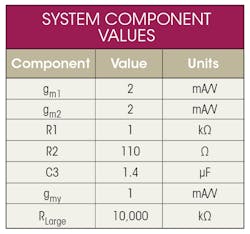
The table lists the component values.
Simulation
To simulate the output impedance, simply ground the inputs and connect an ac current source to the output node. Note that ZOUT = VOUT/IOUT. Since IOUT = 1 (ac source), the magnitude of the output voltage corresponds to the output impedance. By plotting the frequency response, the output impedance can be analyzed.
References
1. G.R. Boyle, “Macromodeling of Integrated Circuit Operational Amplifiers,” IEEE 1974, SC-4
2. M. Alexander, D.F. Bowers, “SPICE Compatible Opamp Macro-Models,” Analog Devices, AN-138 Application Note
3. X. Li, P. Li, Y. Xu, R. Dimaggio, L. Pileggi, “A Frequency Separation Macromodel for System-Level Simulation of RF Circuits,” Design Automation Conference, 2003. Proceedings of the ASP-DAC 2003, p. 891-896
4. “Development of an Extensive SPICE Macromodel for Current-Feedback Amplifiers,” Application Note (SNOA247B), Texas Instruments, May 2013
5. Bruce Carter and Thomas R. Brown, “Handbook of Operational Amplifier Applications,” Application Report (SBOA092A), Texas Instruments, October 2001
Arash Loloee is a member of Texas Instruments’ Group Technical Staff. As a senior IC design engineer, his responsibilities range from designing transistor to system-level projects. He received his PhD in EE and MSEE from Southern Methodist University, as well as his BS in physics from the University of North Texas. He can be reached at [email protected].
Marcos Lopez joined Texas Instruments in 2010 as a modeling engineer after completing several internships with different groups within TI. He received his MSEE form Texas A&M and a BS from the University of Puerto Rico. He can be reached at [email protected].
About the Author
Arash Loloee
Member, Group Technical Staff
Arash Loloee is a member of TI’s Group Technical Staff. As Senior IC Design Engineer, he is responsible for designing transistor- to system-level projects. He received his PhD in EE and MSEE from Southern Methodist University and his BS in physics from the University of North Texas. He also was a lecturer at the University of Texas at Dallas from 2005 to 2011, where he taught various analog-related topics. He has three patents, with one pending. He can be reached at [email protected].
Marcos Lopez
Modeling Engineer
Marcos Lopez joined Texas Instruments in 2010 as a modeling engineer after completing several internships with different groups within TI. He received his MSEE form Texas A&M and a BS from the University of Puerto Rico. He can be reached at [email protected].
Comment About the Article
To join the conversation, and become an exclusive member of Electronic Design, create an account today!

Leaders relevant to this article: