MOSFET Design Basics You Need To Know (Part 1)


What you'll learn:
- MOSFET ABCs.
- MOSFET false turn-on mechanisms.
- Turn-on from excessive source inductance.
Though we’ve been building MOSFETs for more than 40 years, it seems odd that some attributes of the devices still don’t receive the attention they deserve.
Have you ever hard-commutated a MOSFET only to see the element that should be “off” bounce into the “on” condition? Have you ever seen VDS drop to the “on” state when the gate source voltage was in the “off” state? Have you used a MOSFET in linear mode and it failed even though it was within the safe operating area (SOA) limits? Or, have you ever substituted devices for cost, only to find that the newer, more cost-effective devices with similar ratings were failing?
I’d like to delve into these issues by exploring the nuisance dynamic turn-on mechanisms, as well as body-diode reverse recovery, avalanche, and linear-mode operation. Also, I’ll offer suggestions on how to select the proper device and mitigate these issues. A skilled quantum mechanic may find fault with some of my feeble descriptions and drawings, but I will try to make them useful on the bench—where the design ultimately comes together.
Device ABCs: 30 Seconds on Quantum Mechanics
In broad strokes, a MOSFET device allows us to use a relatively low voltage at the gate to modulate current flow from drain to source. Two basic types of MOSFETs are bought as discrete devices today: planar and trench. Other processes previously used just for biCMOS ICs are coming into the discrete market, too, such as lateral MOSFETs (not discussed here).
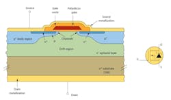
The discrete MOSFET world started with planar devices. The devices are made entirely on a planar process (Fig. 1) with diffused P and N wells, oxide grown on the surface, and surface metallization for the gate and source.
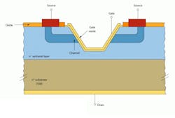
Trench MOSFETs feature higher cell densities, which translates to lower RDS(ON) specifications per unit die size. In a trench device (Fig. 2), the trench is cut into the wafer’s surface, and the gate oxide and metallization are deposited in this trench. The gate field in a trench device exerts influence over a much greater amount of silicon. As a result, the cells can be physically smaller yet yield the same RDS(ON) as planar devices.
The body diode of the MOSFET forms between the n- layer of the MOSFET’s drain and the p+ well of the device’s source. This is the diode depicted in virtually all MOSFET datasheets. In switching applications that use the body diode, the reverse recovery of this PN junction needs to be understood.
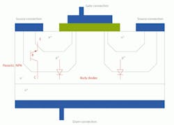
The internal NPN transistor of the MOSFET has its collector at the n- layer in the drain, the base at the source’s P-well, and its emitter in the source’s N-well. Note that the source metallization (Fig. 3) places a very low resistance between the BE junction of this device, making it difficult to turn on.
Capacitive False Turn-On Mechanisms
Several false turn-on mechanisms could create problems in our switching power-supply design. Two capacitive mechanisms top the list. They involve the parasitic device capacitances and transients fast enough to charge and/or discharge them. In most applications, these transients are driven by the instantaneous voltage change across an inductor. This occurs when the converter switches between charging the inductor and discharging, or from the hard switching action when the opposing switch turns on quickly.
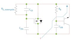
The first mechanism relates to the Miller capacitance of the device (CRSS) interacting with the device’s gate capacitance (CGS). If a fast transient is applied to a device in the off condition, causing the VDS to rise rapidly, the Miller capacitance (Fig. 4) forms a voltage divider with the gate-source capacitance.
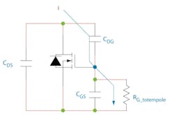
If the device is in the off state, we try to hold this voltage to zero. However, we’ve only got finite impedance to hold the device off. It consists of the sum of the RDS(ON) of the low-side totem pole switch that’s commanding the off state, the off resistance path of the gate-drive series resistance, the internal metallization resistance of the gate (RG), and any parasitic inductance from leads and/or traces.
Because we usually transition quickly (either with an instantaneous change in polarity of an inductor, or with a hard switched capacitive load), this transition’s voltage-change rate is extremely fast. It’s possible that this transient can raise CGS high enough to turn the device on. This problem escalates at higher temperatures, due to decreasing VTH.
Such a concern is no more evident than in a 12- to 1.8-V or lower output-voltage synchronous buck converter with enough load current to keep the output inductor in continuous conduction mode. Remember, in some of these synchronous buck converters, the low-side switch will not turn on unless the output inductor current is in CCM.
In this case, the duty cycle is very small and the low-side switch conducts the load current for the majority of a switching cycle. When the high-side switch turns off, the inductor freewheels and commutates down through the low-side body diode—hopefully for a very short time—then the low-side switch is turned on. The drain-source voltage of the high-side MOSFET then sees a rapid charge from 0 V (on state) to roughly VCC-VF (off state plus freewheel diode).
At this time, the device is very susceptible to false turn-on events. In fact, the probability is so high that we have established figures of merit that compare QGS with QGD; thus, we choose FETs primarily based on this figure. The higher the QGD, the lower the QGS, and the more likely the device will turn on when we don’t want it to in these circumstances. Also, lower RG, lower gate-drive output impedance, and lower trace impedance helps by allowing the device to be held off.
In application, if you suspect there’s a dv/dt turn-on problem, look at VGS, VDS, and ID with the shortest leads and the tightest loops possible. When the low-side switch turns on, you will see a short positive pulse on VGS and an associated drop in VDS. This “switchthrough” condition can be catastrophic.
As a result, you may opt for a device with lower CRSS, higher CISS, and higher threshold (if using logic level). In a really bad case, you could add a little capacitance to the GS terminals and make certain that your driver has a low output impedance as well as minimal RG in the MOSFET.
The second capacitive mechanism relates to the internal NPN transistor buried inside of the MOSFET structure. The BE junction of this device sees a low impedance from the source metallization of the MOSFET, but this metal resistance is non-zero. The Miller capacitance of the NPN transistor is formed by the p-well of the MOSFET and the n- layer in the MOSFET’s drain. A fast transient can couple charge into the BE junction (Fig. 5).
I infrequently see this in applications due to the low resistance of the metal shorting the p-well and the n-well of the MOSFET (BE junction of the buried BJT). Furthermore, the gain of the transistor is designed to be small to further reduce the odds of such a turn-on event.
However, I’ve observed cases in which the gate is pulled well below 0 V, perhaps to –12 V via a gate-drive transformer driving a half-bridge circuit with separate, galvanically isolated, opposed windings for the high- and low-side switches. At these times, when the gate of the high-side switch is first pulled negative and the low-side switch is first turning on, I’ve seen the DS waveform across the high-side switch collapse to the on state, causing switchthrough.
The problem goes away by simply changing the gate drive to an IR2110 or similar device, or perhaps by adding a local PNP transistor to the gate-drive transformer circuit that clamps VGS to zero in the off state. Thus, it can’t be the Miller capacitance of the MOSFET causing the false turn-on. If it were, the false turn-on would worsen with the 0-V off state instead of –12 V. Though it’s rare when the buried NPN turns on, it merits inclusion in a comprehensive discussion of false turn-on mechanisms.
Turn-On from Excessive Source Inductance
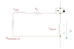
When looking to the structure of most any MOSFET with leads, whether SOIC, DPAK, TO-220, etc., you will see some basic similarities between them. A high-temperature solder connects the substrate of the device to the metal tab. This connection has minimal conductance. Also, heavy bondwires connect the source of the device from the top of the die to the leadframe. Sometimes many parallel bondwires on the source are used for this die-to-leadframe connection (Fig. 6).
The gate is connected from the die to the leadframe with a single smaller bondwire. Problems arise from the source lead’s inductance, though. The source lead is both the “exit point” for the power current path and the return for the on/off current from the gate driver. From a practical standpoint, we can’t truly see the source voltage on leaded parts. The voltage at the source pin is apparent, but the actual source of the device is located a few nanohenries away.
In terms of value, if we consider the base rule of thumb that a single wire, located above a ground plane in free space, will have 20 nH per inch or so of inductance, 3- to 5-nH inductances will prevail for the source connection of MOSFETs with bondwires. Larger packages tend to have larger source inductances.
The inductance in the source tends to oppose both turn-on and turn-off of the device. Usually, turn-off is much more noticeable due to higher currents flowing through the device and the higher energy stored in the source inductance. When we attempt to turn the device off, the source inductance tries to maintain current flow as per V = –Ldi/dt. This means that the polarity of the voltage across the inductor changes instantaneously as the MOSFET interrupts the current flowing through it.
Prior to this event, the voltage drop across the source inductance was positive at the die and negative at the leadframe. After this event, the inductance is negative at the die and positive at the leadframe for a short time.
During this period, this voltage adds to the gate-drive voltage in series. Even though the gate-drive commands the device off through presumably a low-impedance path, the voltage across the source inductance adds to the low voltage that the driver is trying to command. If the voltage is high enough, it will turn the device on in spite of the gate-drive command (Fig. 7).
To fix the problem in high-speed applications, consider leadless packages, especially the copper-clip PQFN devices from International Rectifier, the DirectFET, and the solderable front metal parts. These parts have absolutely minimal source inductance. In applications that require leaded parts, we can pull the gate negative on the off state to help mitigate turn-on from the source inductance.
Originial publish date: April 4, 2010
Updated 07/15/2024

About the Author
Paul Schimel
Senior Field Applications Engineer
Paul Schimel is a senior field applications engineer at International Rectifier. He has more than 15 years experience in power electronics design, EMC, and transformer design including offline ac-dc converters for medium and high power levels, motor drives, and dc-dc converters. He is a hands-on engineer and innovator, endlessly building power electronics circuitry, welding, and machining for audio, HVAC, and propulsion applications. Also, he is a licensed Professional Engineer and holds two patents. He can be reached at [email protected].
Comment About the Article
To join the conversation, and become an exclusive member of Electronic Design, create an account today!

Leaders relevant to this article: