Total power lost due to chip leakage is an increasingly important IC parameter. One of the most common methods of reducing it is to use a multiple-threshold CMOS (MTCMOS) cell to turn the power supply (or ground) off for inactive partitions of the IC. Such a cell (also called a power-switch cell or power-gate cell) can be represented by a PMOS transistor, which turns off the power supply (or NMOS transistor, for ground). They are available in different variations, such as double-row-height standard cells or macros, or as built-in I/Os.
However, there is a “disconnect” between the circuit designers who build these cells and the system-on-chip (SoC) implementation engineers who use them in the design’s floor plan stage. While circuit designers deliver the specifications of these cells with all the details, including on resistance, most SoC designers do not know how to interpret this data.
The challenges include determining the number of power switches needed for a given partition and the optimum placement of these switches. Too few power switches can result in high voltage drop and poor chip performance, while too many such switches can exceed the leakage-power budget.
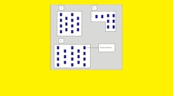
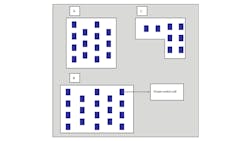
Consider the example floor plan shown in the figure. Partitions A, B, and C are implemented so they can be shut down independently, using different control signals. Also assume, for simplicity’s sake, that the MTCMOS switch cell available is a double-height PMOS header, although this methodology can be applied to any types of switch cells. The challenge is to determine the optimum number of switch cells to be placed inside each of the partitions, under the constraints of chip-leakage power and low voltage-drop objectives.
This floor plan in a low-power design, with the most common configuration of power-switch placement in an array (A, B, and C are partitions of the chip), can be optimized to minimize chip-leakage power dissipation by using a specific methodology.
Typically, power switches are placed as an array, with an x pitch and y pitch, which are predetermined for the entire chip. While this approach is easy to implement, it has no “knowledge” of the power requirement of each partition or of the on resistance of the switch, and it can potentially insert too many switches in some partitions and too few in others.
Instead, designers can consider the power consumption of each partition and estimate the average voltage drop, thereby determining the appropriate number of power switches. Assuming n power switches are placed in partition A, on average, then the current through each of the switches is:
ISwitch = P(A)/(V * n)
where I is the average on-current through the switch, P(A) is power-consumption estimate for partition A, V is the operating voltage, and n is the number of switches for this partition.
The average voltage drop across each power switch is:
IRSwitch = ISwitch * R = P(A) * R/(V * n)
where R is the on resistance of the power switch (usually provided with the circuit specifications). The optimum number of power switches is dictated for partition A by:
n ≥ P(A) * R/(V * IRSwitch)
The IRSwitch can be modeled as a percentage of the overall IR-drop budget (5% of power-supply voltage, for example). This equation shows the minimum number of power switches needed to ensure that partition A does not show a voltage-drop violation. Designers need to perform similar estimates for all the power-down partitions in the full chip. Clearly, the number of power switches for any partition depends on the power consumption (as opposed to its size) and is optimized to limit voltage drop.
To determine the maximum number of power switches for the design, use the power-switch cell-leakage value (usually provided in the specifications):
n(partitions) ≤ total chip switch cell leakage power budget/ switch cell leakage power
Thus, the number of power switches for a given partition in a chip should depend on the power switch’s on resistance and the voltage-drop constraints.

