Enhanced 3D-Printing Technique Yields Custom MEMS Sensors
What you’ll learn:
- Why custom-made sensors using additive manufacturing offers end-user benefits.
- How the AM process was adapted for MEMS sensors.
- The test results of their prototype devices.
MEMS technology in its various implementations has revolutionized sensors over the past few decades, with tiny, highly accurate, low-power/cost devices for sensing acceleration, motion, pressure, and other challenging variables. There’s no need to expound on that success story. Still, there’s an aspect of MEMS devices that can’t be overlooked: While its virtue is that it is inherently a high-volume, (mostly) silicon-based fabrication technology, these same attributes make it a poor fit for unique, single- or low-quantity, custom sensors.
Along a similar timeline, the very different technology of additive manufacturing (AM, commonly called 3D printing) has radically changed the way that custom-designed components can be built using a range of metals, polymers, and other specialty materials. With 3D printing, a design that exists on a computer screen via a CAD package can be fabricated “on the spot” and is especially well-suited for one-off or low-volume production runs.
The problem is that these two are at opposite ends of the volume and customization spectrum. But what if you could use 3D printing to create and build a one-off custom-designed MEMS sensor as needed, thus giving you the best of both worlds?
Two-Photon Polymerization
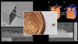
Yet that’s what a team at the KTH Royal Institute of Technology in Stockholm (Sweden) has done (Fig. 1). The researchers built on a process called two-photon polymerization, which can produce high-resolution objects as small as few hundreds of nanometers in size, but not capable of sensing functionality.
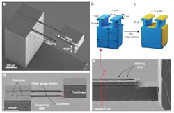
To form the transducing elements, the method uses a technique called shadow-masking, which works something like a stencil. On the 3D-printed structure, they fabricated features with a T-shaped cross-section that work like umbrellas. They then deposited metal from above, and as a result, the sides of the T-shaped features aren’t coated with the metal. This means the metal on the top of the T is electrically isolated from the rest of the structure.
Prof. Frank Niklaus, who led the research team, noted, “This is something that has not been possible until now, because the startup costs for manufacturing a MEMS product using conventional semiconductor technology are on the order of hundreds of thousands of dollars and the lead times are several months or more. The new capabilities offered by 3D-printed MEMS could result in a new paradigm in MEMS and sensor manufacturing."
He added that “scalability [in volume] isn’t just an advantage in MEMS production, it’s a necessity. This method would enable fabrication of many kinds of new, customized devices.”
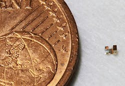
They printed the accelerometer structure on a glass substrate, with a supporting pillar having two single-sided, clamped horizontal cantilevers and a proof mass attached at the end of the two cantilevers (Fig 2). The design freedom offered by the 3D-printing process allowed them to pattern shadow-masking structures with T-shaped cross-sections on top of the cantilevers and the supporting pillar to define the areas of the strain-gauge transducers, the electrical interconnects, and the probing electrodes.
Test Setup and Results
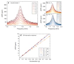
To assess performance, the team conducted a range of tests using a fairly standard arrangement that included a laser Doppler vibrometer (Fig. 3). The piezoshaker driving frequency was swept between 1.4 and 2 kHz, with voltage amplitudes ranging from 1 to 7 VRMS.
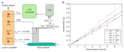
They conducted both mechanical and electrical tests, although the two aspects are related. The mechanical characterization assessed factors such as the material and stress/strain performance, which was compared to their COMSOL models (there was close agreement).
The electrical characterization assessed parameters such as relative resistance change (ΔR/R) as measured at different frequencies and driving voltages of the piezoshaker on the accelerometer (Fig. 4). They also tested stability over a 10-hour period, as even a “perfect” sensor is of little use if it drifts over time (in contrast, temperature-based variations can often be accommodated or compensated, but time-related drift is more difficult to accept).
The work is detailed in their readable 13-page paper “Micro 3D printing of a functional MEMS accelerometer” published in Nature Microsystems & Nanoengineering; there’s also a 13-page Supplemental file available. If those two resources aren’t enough to satisfy your interest in their work, you can also read the 100-page doctoral thesis “Additive Manufacturing and Integration of 3D MEMS using Ultrafast Lasers and Magnetic Assembly” by one of the authors, on which much of the work is based.
About the Author

Bill Schweber
Contributing Editor
Bill Schweber is an electronics engineer who has written three textbooks on electronic communications systems, as well as hundreds of technical articles, opinion columns, and product features. In past roles, he worked as a technical website manager for multiple topic-specific sites for EE Times, as well as both the Executive Editor and Analog Editor at EDN.
At Analog Devices Inc., Bill was in marketing communications (public relations). As a result, he has been on both sides of the technical PR function, presenting company products, stories, and messages to the media and also as the recipient of these.
Prior to the MarCom role at Analog, Bill was associate editor of their respected technical journal and worked in their product marketing and applications engineering groups. Before those roles, he was at Instron Corp., doing hands-on analog- and power-circuit design and systems integration for materials-testing machine controls.
Bill has an MSEE (Univ. of Mass) and BSEE (Columbia Univ.), is a Registered Professional Engineer, and holds an Advanced Class amateur radio license. He has also planned, written, and presented online courses on a variety of engineering topics, including MOSFET basics, ADC selection, and driving LEDs.
Comment About the Article
To join the conversation, and become an exclusive member of Electronic Design, create an account today!

Leaders relevant to this article: