Check out Electronic Design's coverage of GTC 2024.
NVIDIA pushes the boundaries of AI silicon with its next generation of “Blackwell” GPUs.
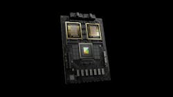
The Santa Clara, Calif.-based company rolled out its new flagship GPU, the B200. Based on its Blackwell architecture, NVIDIA said the B200 is 4X faster for training than its predecessor, the Hopper GPU, while offering an even larger boost to AI inferencing, up to 30X. The B200 is the company’s first chiplet-based design, bringing even more computational power to the table at 25X better energy efficiency.
Revealed at NVIDIA’s developer conference, GTC 2024, the GPU architecture is named in honor of the mathematician David Harold Blackwell, the first Black inductee into the U.S. National Academy of Sciences.
NVIDIA said the higher performance unlocked by Blackwell gives companies at the forefront of the AI boom the ability to train and run larger, more intricate AI models at a fraction of the cost. These include transformer-based models such as OpenAI's GPT-4, Google’s Gemini, and Meta's Llama. These high-end models—also called large language models (LLMs)—tend to have more than 100 billion parameters, scaling up to trillions of these building blocks in the future, thus straining the limits of GPUs and other AI chips.
Stated Ian Buck, NVIDIA’s head of high-performance computing and hyperscale, "Blackwell is a new class of Al superchip.” The B200 is manufactured using a custom 4-nm N4P process technology from TSMC.
He said innovations to everything from the processor cores to connectivity and memory in the Blackwell GPUs open the door to training and real-time inference for models containing up to 10 trillion parameters.
The B200 consists of a pair of silicon die manufactured at the reticle limit—or the maximum area that a single chip can be made using modern process technology, which is currently around 800 mm2. The chiplets are united in the same package using a 10-TB/s memory-coherent chip-to-chip connection so that they act as a single AI accelerator measuring about 1600 mm2. The B200 is equipped with 208 billion transistors in all.
The B200 is bordered on the package by high-bandwidth memory (HBM) stacked on the same package, totaling 192 GB of enhanced HBM3E, up from 141 GB in the second-generation Hopper GPU, the H200. More memory means that larger machine-learning (ML) models—or larger portions of AI models—can fit within a single GPU, saving power that would usually be wasted by accessing outside memory.
The memory bandwidth clocks in at 8 Tb/s, up from 4.8 Tb/s in the most advanced Hopper GPU. High memory bandwidth is increasingly vital as it reduces latency to the levels required for AI training and inferencing.
Transformer Engine: The Key to the Blackwell GPU
Upgrading the underlying silicon and surrounding it with more advanced memory are not behind all of the performance gains in the B200. The innovations that make the biggest impact stem from the new Blackwell architecture itself.
“A new type of AI is emerging, one that is even more intelligent, one that has been built not from a single AI model, but from a collection of AI models,” said Buck. “For every layer of a transformer, they are sharing their information to decide which one has the best answer for the next layer to build even more intelligent models. This allows AI to scale further—to trillion-parameter models—that we have never seen before.”
“The challenge of that is computing,” said Buck, adding that “as models are getting larger, training takes more computing. Also, inference is becoming a bigger and bigger part of the challenge.”
According to Buck, to tackle these challenges, the “transformer engine” is being upgraded at the core of the Blackwell GPU. Introduced as its Hopper GPU, this engine evaluates every layer in the neural network and the tensors used to represent them. As the GPU trains or runs the ML model over time, it decides whether it makes sense to carry out AI computations using smaller numbers with less precision. Hopper uses floating-point numbers as small as 8 bits (FP8) instead of being limited to 16-bit floating point (FP16).
Using smaller numbers to handle the computations behind AI enables faster execution, specifically for inference. Reducing precision also makes it possible for larger, more complex AI models—as in, the number of parameters—to fit into the memory of a single GPU.
The transformer engine in Blackwell pushes the envelope even further. The GPU uses what NVIDIA calls “micro-tensor scaling” to improve performance and accuracy to the point where it can run the computations at the heart of Al using floating-point numbers only 4 bits wide (FP4), which is boon for AI inference. “That means we can deliver twice the amount of compute as before, we can double the effective bandwidth, and we can double the model size that can fit on an individual GPU,” said Buck.
The transformer engine inside the Blackwell GPU is also very fine-grained, said Buck. It can scale the numbers used by even smaller building blocks inside the tensors themselves, instead of the entire tensor.
"Getting down to that level of fine granularity is a miracle in itself," noted Buck. The B200 GPU can pump out up to 10,000 trillion operations per second (10 petaFLOPS) using the FP8 format. That translates to 2.5X faster inferencing than the Hopper GPUs that it released in 2022. Buck added that Blackwell-based GPUs can increase their performance up to 20 petaFLOPS when using the more compact FP4 format for inference.
NVIDIA said Blackwell adds “confidential computing” capabilities that keep AI models and data used for training them secure, which is valuable in sectors such as healthcare and finance, where privacy matters.
One of the unfortunate tradeoffs with Blackwell is its power consumption. The B200 burns through 1000 W (1 kW), and the B100 fits into the same 700-W power envelope (TDP) as its predecessor. Designing a power delivery network (PDN) that can supply enough power to AI accelerators like those from NVIDIA is becoming a daunting task, as is dissipating the heat that the chips generate.
High-Bandwidth Connectivity: The Missing Link in AI
The B200 itself is only one piece of the puzzle. High-bandwidth, low-latency connectivity is a must-have for building colossal AI systems that can train and run massive AI models behind the boom in generative AI.
NVIDIA uses the new generation of its chip-to-chip interconnect technology, NVLink, to lash together the silicon die in a package. In addition, the chips act as a single unified GPU to the software that runs on top of it, instead of a pair of GPUs placed beside each other. NVLink is also used to bridge longer distances in data centers, allowing high-speed communication between up to 576 GPUs.
Blackwell leverages the NVLink interconnect to transfer data at up to 1.8 Tb/s in both directions between other GPUs in the system, doubling the bandwidth of the NVLink in Hopper, according to the company.
Also revealed at GTC is that the Blackwell GPU adds another engine to run diagnostics and test for potential reliability risk. The new engine uses AI-based preventative maintenance at the chip level that can monitor “every single gate and every bit of memory on the chip and connected to it” and identify any weak points. The objective is to increase uptime and improve resiliency for large-scale systems that tend to run uninterrupted for weeks or months at a time to train the largest ML models.
While it’s the dominant force in the world of AI silicon, NVIDIA is trying to stay a step ahead of rivals Intel (with its Gaudi 2 and future Gaudi 3 accelerators) and AMD (with its Instinct GPUs). It’s also contending with cloud giants such as AWS, Google, and Microsoft, which are rolling out in-house AI silicon for training and inferencing. On top of that, Cerebras Systems and many other startups are trying to close the gap with NVIDIA.
The company is out to fend off the competition with its new Blackwell GPUs. To make it happen, plans are to package them with a broad range of connectivity and software technologies into supercomputer-class systems.
The Blackwell GPUs are also at the heart of the company’s new GB200 "superchips." These are modules that connect its “Grace” Arm CPU and a pair of the Blackwell GPUs over a 900-GB/s NVLink interconnect.
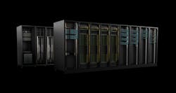
The modules are arranged into larger computing modules, called the DGX GB200. Up to eight of these units can be linked with NVLink to create a supercomputer-class system called a SuperPOD that contains 576 Blackwell chips.
SuperPODs can run up to 11.5 exaFLOPS at FP4 precision, delivering 30X more performance than the H100 for inferencing, said NVIDIA. Uniting tens of thousands of GPUs in a system is doable using the company’s InfiniBand networking technology.
These “AI supercomputers are the factories of the AI industrial revolution,” said CEO Jensen Huang.


