Power modules range from heavy-duty IGBTs, thyristors, and GTOs down to relatively low-power IGBT discretes and MOSFETs. Their applications range from rail traction, welding, and marine applications at the high end down to audio and video equipment and kitchen appliances at the low end. Before the power modules are used in the assembly of a system, it is worthwhile to learn whether the modules contain internal structural defects that could cause the module to fail while in operation.
Because of their roles in regulating power, all these modules have a common requirement: During their anticipated service life, they need to dissipate enough of the heat generated by the die to keep the die from overheating and failing. IGBT modules are in a separate class in this regard, and the remaining power modules are discussed here.
Before the power modules are used in the assembly of a system, it is worthwhile to learn whether internal structural defects can cause the module to fail while in operation. The greatest concern in power modules is the presence of an internal gap, which may be more specifically described as a delamination, a non-bond, a crack, or a void. All of these are gaps that contain air, or, depending on the manufacturing processes used, another gas such as nitrogen. The basic problem is that gas-filled gaps are very efficient blockers of heat flow. One or more gaps between the die and the heat sink can cause the diet to overheat and fail, particularly when, as is the case with many power modules, the heat-dissipation design of the module has little room for error.
Gap-type defects can be found by destructive physical analysis (sectioning and polishing) of the power module. This method may demonstrate that the method used to fabricate the module needs modification to avoid gap-type defects, but the module examined is no longer usable. The chief method for finding gap-type defects without destruction is acoustic micro imaging. An acoustic micro-imaging tool pulses ultrasound into the module and receives echoes from internal features. X-ray cannot image delaminations because the delaminations are much too thin. The ultrasound used in acoustic micro imaging, though, is virtually 100% reflected by gaps—even gaps as thin as 100Å (0.0003937 inch). Gaps are very efficient blockers of heat, but they are even more efficient at reflecting the ultrasound that reveals the presence of gaps and images them.
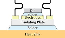
Thyristors, GTOs, and IGBT modules share a similar overall architecture, having several layers (Fig. 1). The die is at top. Heat travels downward through intervening layers to reach the heat sink at the bottom. The heat sink may be considerably wider than the rest of the module and have a hole at either end for bolting the module to an even larger heat sink. The die typically has at least three leads. Where current levels are higher, it may have more than three. The leads are far more robust than the wires used in, for example, plastic-encapsulated microcircuits. The die sits atop one of the electrodes and is usually encapsulated with silicone to prevent moisture damage.
Gaps of various kinds are the most common defects in these power modules. There may be a delamination between the die and the solder, or there may be voids (air bubbles) in the solder. The same types of gaps may be present between the insulating plate and the heat sink. The next most frequent defect is probably variation in the thickness of a solder layer. This variation can cause uneven thermal dissipation across the die and can result in stresses in the die. Even without delaminations or voids, thickness variation across a solder layer can diminish thermal dissipation. It can be imaged acoustically because echoes from different points on the slanted interface arrive at the transducer at different times.
There are a few other defect types in these modules. A tab-style lead, for example, may have only a partial bond to the die, or it may have no bond at all. But compared to other device types, and particularly to PEMs, the number of defect types is small.
To image internal features, the scanning transducer used by an acoustic micro imaging tool such as a Sonoscan C-SAM system pulses ultrasound into one surface of a power module. Because ultrasound does not travel through air, the pulse is coupled to the surface of the power module by a water column that travels with the transducer. The pulse typically travels through solid materials at thousands of meters per second, the exact figure depending on the material. The bulk of a homogeneous material (silicon, copper, ceramic, solder, etc.) having no defects will send back no echoes. Echoes are returned only by the interfaces between materials. The interface between two solids typically returns between 20% and 80% of the ultrasound. The interface between a solid and a gap (air) returns very nearly 100%. The echoes from solid-solid interfaces are of low to moderate amplitude, while the echoes from solid-air interfaces are of high amplitude. In a monochromatic image, these high-amplitude echo signals are bright white, but for viewing they may be changed to any other color. Lower-amplitude echoes are some shade of gray, but may also be altered.
PEMs are imaged from the top side; that is, the transducer scans the top surface of the package and sends pulses through the encapsulant into the package. IGBT modules are typically imaged from the heat-sink side before encapsulation, because the top side is very sensitive to water. Scanning the bottom side of samples was not possible until Sonoscan invented an inverted transducer, accompanied by an inverted water column that scans the bottom side of IGBTs and other samples while leaving the top side dry.
Figure 2 is the acoustic image of one of three die in a discrete power device. The image shows the die attach layer, and was made by scanning the heat sink at the bottom of the device. A glance at Fig. 1 shows that the ultrasound traveled through the heat sink and other material layers to reach the die attach. At each bonded material interface, some of the pulsed ultrasound is reflected, and some crosses the interface and travels to the next interface, where a similar reflection/transmission event occurs. Echoes come back to the transducer from all of the material interfaces, but to make this image the echoes were gated on the die attach layer—meaning that echoes from all other depths were ignored in making the image.
Gray and black parts of the image indicate that the die attach material is well bonded in those regions. The numerous small red and yellow features in the die attach are voids, which reduce the area of bonding and block heat dissipation. Depending on the total area they cover, these voids might not be a cause for rejection of this device from assembly. But voids are often capable of increasing their effective size as a result of thermal cycling during service. The rate of heat dissipation from this die might gradually shrink until failure occurs.
MOSFETs and other power devices tend to resemble plastic-encapsulated microcircuits more than they resemble larger power devices. They also handle lower power loads and operate at higher frequencies. But being power devices, they need to dissipate heat effectively, and typically have a heat sink to which the die is bonded.
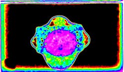
A TO-220 device is imaged in Fig. 3. The general structure of the device—mold compound, die, die attach, substrate—is much like the structure of PEMs. To make this image, the surface of the heat sink was scanned, and the echoes were gated on the solder bond between the die and the heat sink. The image shows small defects as well as the outline of the rectangular die, and also tells the history of the bonding procedure.
The pink oval at the center is the outline of the fluid solder that was initially placed on the heat sink. The solder cooled slightly before the die was placed. Placement of the die caused the solder to spread outward to and beyond the edges of the rectangular die. Die placement also introduced small black voids, most of which lie just beyond the edges of the pink region. These voids are probably too small and too few to significantly block heat dissipation in a low-power device.
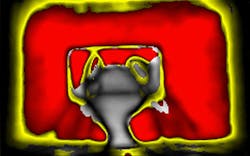
Figure 4 is the acoustic image of a TO-220 that was imaged through the top surface of the component package. The return echoes were gated on the depth of the die; echoes from other depths were ignored.
The more or less rounded gray area represents good bonding between the mold compound and part of the die (above the horizontal dark line across the gray area) and between the mold compound and a small part of the heat sink. The other regions of the die and heat sink are red, meaning that they are not bonded. This TO-220 package would be very likely to overheat because its heat dissipation path is highly compromised.
Because the return echoes were gated on the depth of the die, the leads attached to the die are not directly visible. But as the echoes returned to the transducer, they were locally blocked by the wires, which show up as dark acoustic shadows to the right and left of the gray well bonded area.
Contact information:
Sonoscan, Inc.
2149 E. Pratt Blvd.
Elk Grove Village IL USA 60007
Phone: 847 437-6400
Fax: 847 437-1550
E-mail: [email protected]
Website: www.sonoscan.com


